Introduction to PCB Vias
Printed Circuit Boards (PCBs) are essential components in modern electronics, providing a platform for interconnecting electronic components. One crucial aspect of PCB design is the use of vias, which are conductive pathways that allow electrical signals to pass through different layers of a multi-layer PCB. In this comprehensive article, we will explore the various types of PCB vias, their design considerations, and the methods used for covering them.
What are PCB Vias?
PCB vias are small holes drilled through a printed circuit board that are subsequently plated with a conductive material, typically copper. These conductive pathways enable electrical signals to travel between different layers of a multi-layer PCB, allowing for more complex routing and efficient use of board space. Vias play a crucial role in PCB design, as they facilitate the interconnection of components and traces on different layers of the board.

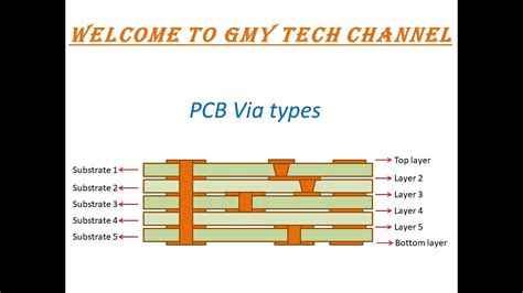
Types of PCB Vias
There are several types of PCB vias, each with its own characteristics and applications. The most common types include:
Through-hole Vias
Through-hole vias are the most basic type of via, extending through all layers of the PCB. They are created by drilling a hole through the entire board and plating it with a conductive material. Through-hole vias are reliable and provide strong mechanical connections, making them suitable for components that require high current carrying capacity or are subject to mechanical stress.
Blind Vias
Blind vias are a type of via that starts on an outer layer of the PCB and terminates on an inner layer, without extending through the entire board. Blind vias are used to connect an outer layer to one or more inner layers, allowing for more efficient use of board space and reducing the overall size of the PCB.
Buried Vias
Buried vias are similar to blind vias, but they are located entirely within the inner layers of the PCB, without extending to either outer layer. Buried vias are used to interconnect inner layers of the board, providing more flexibility in routing and enabling higher component density.
Micro Vias
Micro vias are small, laser-drilled vias that are typically used in high-density interconnect (HDI) PCBs. These vias have a diameter of less than 150 microns and are used to connect fine-pitch components or to create high-density routing in small areas of the board.
Stacked Vias
Stacked vias are a combination of blind or buried vias that are aligned vertically in the PCB stackup. This arrangement allows for the creation of longer conductive paths through the board, enabling more complex routing and higher component density.

PCB Via Design Considerations
When designing PCB vias, several factors must be taken into account to ensure optimal performance and reliability:
Via Size and Aspect Ratio
The size of a via is determined by its diameter and the thickness of the PCB. The aspect ratio, which is the ratio of the via’s depth to its diameter, is an essential consideration in via design. A high aspect ratio can make it difficult to achieve reliable plating, while a low aspect ratio may result in larger vias that consume more board space.
Via Placement and Spacing
The placement and spacing of vias on a PCB are critical factors in ensuring signal integrity and preventing electromagnetic interference (EMI). Vias should be placed strategically to minimize the length of conductive paths and to avoid interfering with other components or traces on the board.
Via Impedance Matching
In high-speed PCB designs, it is essential to match the impedance of the vias to that of the traces to minimize reflections and ensure signal integrity. This can be achieved by adjusting the size and spacing of the vias, as well as by using impedance-controlled materials and design techniques.
Thermal Management
Vias can also play a role in thermal management, as they can be used to transfer heat from components to other layers of the PCB or to external heat sinks. Thermal vias, which are filled with a thermally conductive material, can be used to enhance heat dissipation in high-power applications.

PCB Via covering
After vias are drilled and plated, they are often covered to protect them from environmental factors and to improve the aesthetics of the PCB. There are several methods for covering PCB vias:
Solder Mask
Solder mask is a polymer coating that is applied to the surface of the PCB, covering the vias and other exposed copper areas. The solder mask protects the vias from oxidation and prevents solder bridging during the assembly process. Solder mask is available in various colors and can be used to create text, logos, or other markings on the PCB.
Via Filling
Via filling involves filling the vias with a non-conductive material, such as epoxy or resin, to create a smooth, planar surface. This technique is often used in high-density PCBs to prevent solder from wicking into the vias during the assembly process, which can cause component misalignment or other defects.
Via Capping
Via capping is a process in which a thin layer of conductive material, such as copper or gold, is applied over the top of the via to seal it and provide additional protection. Via capping can also be used to improve the electrical and thermal performance of the via, as well as to enhance its compatibility with certain surface finishes or assembly processes.
FAQ
1. What is the difference between a through-hole via and a blind via?
A through-hole via extends through all layers of the PCB, while a blind via starts on an outer layer and terminates on an inner layer, without going through the entire board.
2. What is the purpose of a micro via?
Micro vias are small, laser-drilled vias used in high-density interconnect (HDI) PCBs to connect fine-pitch components or create high-density routing in small areas of the board.
3. Why is via impedance matching important in high-speed PCB designs?
Via impedance matching is crucial in high-speed PCB designs to minimize reflections and ensure signal integrity. Mismatched impedances can lead to signal distortion and decreased performance.
4. What is the role of solder mask in via covering?
Solder mask is a polymer coating applied to the surface of the PCB, covering vias and other exposed copper areas. It protects the vias from oxidation and prevents solder bridging during the assembly process.
5. What are the benefits of via filling?
Via filling involves filling vias with a non-conductive material to create a smooth, planar surface. This technique prevents solder from wicking into the vias during the assembly process, which can cause component misalignment or other defects. Via filling is particularly useful in high-density PCBs.
Conclusion
PCB vias are essential components in modern electronics, enabling the interconnection of components and traces on different layers of a multi-layer PCB. Understanding the various types of vias, their design considerations, and the methods used for covering them is crucial for creating reliable, high-performance PCBs. By carefully considering factors such as via size, placement, impedance matching, and thermal management, designers can optimize their PCB Layouts and ensure the best possible performance for their electronic devices.
No responses yet