Introduction to PCB Vias
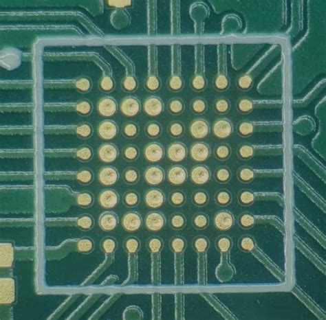
A printed circuit board (PCB) via is a small hole drilled through a PCB that electrically connects different layers of the board. Vias allow signals and power to be routed between layers, enabling more compact and complex PCB designs. They are essential features in multi-layer PCBs widely used in modern electronics.
Key Characteristics of PCB Vias
- Small holes drilled through a PCB, typically 0.1-1.0mm in diameter
- Electroplated with conductive material, usually copper, to create electrical connections between layers
- Enable routing signals and power between layers of a multi-layer PCB
- Allow for more compact and complex board designs compared to single-layer PCBs
- Different types of vias (through-hole, blind, buried) are used depending on the PCB design requirements
Types of PCB Vias
There are three main types of PCB vias, each with specific characteristics and applications:
Through-Hole Vias
- Most common type of via
- Drilled completely through the PCB, connecting all layers
- Provides strong mechanical connection and high current carrying capacity
- Typically used for through-hole components and in high-power applications
- Can be filled with conductive or non-conductive material for improved strength and thermal management
Blind Vias
- Drilled from one surface of the PCB to an inner layer, but not through the entire board
- Used to connect an outer layer to one or more inner layers
- Allows for higher density routing and more compact board designs
- Typically smaller in diameter than through-hole vias
- More expensive to manufacture than through-hole vias due to additional processing steps
Buried Vias
- Drilled between inner layers of the PCB, not visible from either surface
- Used to connect two or more inner layers without using space on the outer layers
- Enables even higher density routing and more complex board designs
- Most expensive type of via to manufacture, requiring precise layer alignment and multiple drilling/plating steps
- Often used in high-density interconnect (HDI) PCBs for advanced applications
| Via Type | Description | Connects | Manufacturing Cost |
|---|---|---|---|
| Through-Hole | Drilled through entire PCB | All layers | Low |
| Blind | Drilled from surface to inner layer(s) | Outer to inner layer(s) | Medium |
| Buried | Drilled between inner layers | Inner layers only | High |

Via Manufacturing Process
The manufacturing process for PCB vias involves several key steps:
-
Drilling: Holes are drilled through the PCB substrate at the designated via locations using automated drilling machines. The drill bit size determines the via diameter.
-
Deburring: After drilling, the via holes are cleaned to remove any debris or burrs that could interfere with the plating process.
-
Electroless copper deposition: A thin layer of copper is chemically deposited onto the walls of the via holes, providing a conductive surface for the subsequent electroplating step.
-
Copper electroplating: The via holes are electroplated with a thicker layer of copper, typically 1-25 µm, to achieve the desired electrical and mechanical properties. This step ensures reliable connections between layers.
-
Filling (optional): For some applications, via holes may be filled with conductive or non-conductive material to improve mechanical strength, thermal management, or signal integrity. Conductive filling materials include copper paste, silver paste, and solder, while non-conductive fillers include epoxy resins.
-
Planarization (optional): If vias are filled, the PCB surface may need to be planarized by sanding or chemical mechanical polishing (CMP) to remove any excess fill material and ensure a flat surface for subsequent processing steps.

Via Design Considerations
When designing PCBs with vias, several key factors must be considered to ensure optimal performance and manufacturability:
Via Size and Spacing
- Via diameter should be as small as possible to minimize board space usage, but large enough to ensure reliable manufacturing and electrical performance
- Minimum via size is limited by the PCB manufacturer’s drilling capabilities and the required current carrying capacity
- Via spacing should be sufficient to prevent electrical shorts and maintain signal integrity, typically at least 2-3 times the via diameter
Via Aspect Ratio
- The ratio of via depth to diameter, known as the aspect ratio, should be within the PCB manufacturer’s capabilities
- High aspect ratio vias (>10:1) are more challenging to manufacture reliably and may require specialized processes or materials
- Low aspect ratio vias (<5:1) are easier to manufacture but may limit the number of layers that can be interconnected
Via Positioning
- Vias should be placed strategically to minimize signal path lengths and reduce electromagnetic interference (EMI)
- Avoid placing vias too close to component pads or other features that could interfere with soldering or assembly
- Consider the impact of via placement on the overall PCB layout and routing strategy
Signal Integrity
- High-speed signals are sensitive to via geometry and positioning, as vias can introduce impedance discontinuities and reflections
- Use controlled impedance vias or via stubs to match the impedance of the signal traces and reduce reflections
- Minimize the number of vias in high-speed signal paths to reduce the potential for signal degradation

Via Reliability and Testing
Ensuring the reliability of PCB vias is critical for the overall performance and longevity of electronic devices. Several testing methods are used to verify via integrity:
Continuity Testing
- Checks for electrical continuity between layers connected by vias
- Can be performed using flying probe or bed-of-nails testing equipment
- Helps identify open circuits or high-resistance connections caused by manufacturing defects
Cross-Sectioning
- Destructive test method that involves cutting the PCB and examining the via cross-section under a microscope
- Allows for visual inspection of via plating thickness, uniformity, and any defects such as voids or cracks
- Typically performed on a sample basis as part of process validation or failure analysis
Thermal Stress Testing
- Subjects the PCB to temperature cycling or thermal shock to simulate real-world operating conditions
- Helps identify via failures caused by thermal expansion mismatches or poor plating adhesion
- Can be combined with electrical testing to monitor via performance over time
Accelerated Life Testing
- Applies elevated stress levels (e.g., temperature, humidity, voltage) to accelerate the aging process
- Helps predict long-term via reliability and identify potential failure modes
- Results can be used to improve via design or manufacturing processes for enhanced durability
By conducting these tests and implementing appropriate design and manufacturing controls, PCB manufacturers can ensure the reliability and performance of vias in a wide range of applications.
Advanced Via Technologies
As PCB technology continues to evolve, advanced via technologies are being developed to enable even greater design flexibility and performance:
Microvias
- Extremely small vias, typically less than 150 µm in diameter
- Used in high-density interconnect (HDI) PCBs for compact, high-performance electronics
- Can be stacked or staggered to create dense interconnect structures
- Require specialized manufacturing processes, such as laser drilling or plasma etching
Conductive Ink Vias
- Created by printing conductive ink into via holes instead of electroplating
- Enables the creation of vias in flexible or stretchable PCBs
- Allows for faster and more cost-effective prototyping and low-volume production
- Limited to lower current carrying capacity compared to electroplated vias
Embedded Vias
- Vias that are completely embedded within the PCB substrate, not visible from either surface
- Created by drilling and plating vias in individual PCB layers before lamination
- Allows for even greater routing density and design flexibility
- Requires precise layer alignment and specialized lamination processes
As these advanced via technologies continue to mature, they will enable the development of even more complex and high-performance electronic devices in the future.
Frequently Asked Questions (FAQ)
- What is the difference between a through-hole via and a blind via?
-
A through-hole via is drilled completely through the PCB, connecting all layers, while a blind via is drilled from one surface of the PCB to an inner layer, but not through the entire board. Blind vias allow for higher routing density and more compact designs, but are more expensive to manufacture than through-hole vias.
-
Can vias be used for thermal management in PCBs?
-
Yes, vias can be used for thermal management by providing a path for heat to dissipate from components to other layers or to a heatsink. Thermal vias are often filled with a conductive material, such as copper or silver paste, to enhance their thermal conductivity.
-
What is the minimum size of a via that can be manufactured?
-
The minimum via size depends on the PCB manufacturer’s capabilities and the specific application requirements. Typically, the smallest vias are around 0.1-0.2mm in diameter, but advanced technologies like microvias can be even smaller, down to 0.05mm or less.
-
How do vias affect signal integrity in high-speed PCBs?
-
Vias can introduce impedance discontinuities and reflections in high-speed signal paths, leading to signal degradation. To minimize these effects, designers can use controlled impedance vias, reduce the number of vias in critical signal paths, and optimize via placement and geometry.
-
What is the purpose of via filling, and when is it necessary?
- Via filling is the process of filling via holes with a conductive or non-conductive material to improve mechanical strength, thermal management, or signal integrity. Conductive filling is often used in high-current applications or to enhance thermal dissipation, while non-conductive filling can improve mechanical stability and prevent solder wicking during assembly. Via filling is typically necessary when the PCB design requires enhanced performance in these areas.
Conclusion
PCB vias are essential components in modern electronic devices, enabling the creation of compact, multi-layer PCBs with complex interconnect structures. By understanding the different types of vias, their manufacturing processes, and design considerations, engineers can create high-performance PCBs that meet the demands of increasingly sophisticated applications. As via technologies continue to advance, we can expect to see even more innovative and powerful electronic devices in the future.
No responses yet