Introduction to PCB Stackup
PCB stackup refers to the arrangement of layers in a printed circuit board (PCB). It is a critical aspect of PCB design, as it determines the electrical properties, mechanical strength, and manufacturability of the board. A well-designed PCB stackup ensures proper signal integrity, reduces electromagnetic interference (EMI), and minimizes manufacturing issues.
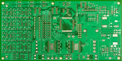
In this article, we will discuss the standard stackup for Multilayer PCBs used by RAYPCB, a leading PCB manufacturer. We will cover the different types of layers, their functions, and the considerations for designing an optimal PCB stackup.
Types of Layers in a PCB Stackup
A typical PCB stackup consists of the following types of layers:
Signal Layers
Signal layers are used for routing the electrical signals between components on the PCB. They are typically made of copper and are etched with the desired trace patterns. The number of signal layers in a PCB depends on the complexity of the design and the required functionality.
Ground Layers
Ground layers are used to provide a low-impedance return path for the electrical signals. They also help in reducing EMI and crosstalk between signals. Ground layers are usually placed adjacent to signal layers to minimize the loop area and provide effective shielding.
Power Layers
Power layers are used to distribute the power supply to different parts of the PCB. They are typically placed near the center of the stackup to minimize the voltage drop and provide a stable power supply to the components. Power layers also help in reducing EMI by providing a low-impedance path for the return currents.
Dielectric Layers
Dielectric layers are used to insulate the conductive layers from each other. They are made of non-conductive materials such as FR-4, Rogers, or Isola. The thickness and material of the dielectric layers affect the electrical properties of the PCB, such as the characteristic impedance and the propagation delay.

RAYPCB Standard Stackup for Multilayer PCBs
RAYPCB offers a standard stackup for multilayer PCBs that ensures optimal performance and manufacturability. The stackup is designed to meet the requirements of a wide range of applications, from high-speed digital to RF and microwave designs.
4-Layer PCB Stackup
The standard 4-layer PCB stackup used by RAYPCB is as follows:
| Layer | Material | Thickness (mm) | Function |
|---|---|---|---|
| 1 | Copper | 0.035 | Signal |
| 2 | FR-4 | 0.2 | Core |
| 3 | Copper | 0.035 | Ground |
| 4 | FR-4 | 0.2 | Core |
| 5 | Copper | 0.035 | Power |
| 6 | FR-4 | 0.2 | Core |
| 7 | Copper | 0.035 | Signal |
This stackup provides a good balance between signal integrity and manufacturability. The signal layers are placed on the outer layers to minimize the dielectric thickness and improve the trace impedance control. The ground and power layers are placed adjacent to the signal layers to provide effective shielding and reduce EMI.
6-Layer PCB Stackup
For more complex designs, RAYPCB offers a standard 6-layer PCB stackup:
| Layer | Material | Thickness (mm) | Function |
|---|---|---|---|
| 1 | Copper | 0.035 | Signal |
| 2 | FR-4 | 0.2 | Core |
| 3 | Copper | 0.035 | Ground |
| 4 | FR-4 | 0.2 | Core |
| 5 | Copper | 0.035 | Signal |
| 6 | FR-4 | 0.2 | Core |
| 7 | Copper | 0.035 | Power |
| 8 | FR-4 | 0.2 | Core |
| 9 | Copper | 0.035 | Ground |
| 10 | FR-4 | 0.2 | Core |
| 11 | Copper | 0.035 | Signal |
This stackup provides more flexibility in routing and better signal integrity. The additional signal layers allow for more complex routing, while the multiple ground and power layers provide better shielding and power distribution.
8-Layer PCB Stackup
For high-density designs with demanding signal integrity requirements, RAYPCB offers an 8-layer PCB stackup:
| Layer | Material | Thickness (mm) | Function |
|---|---|---|---|
| 1 | Copper | 0.035 | Signal |
| 2 | FR-4 | 0.2 | Core |
| 3 | Copper | 0.035 | Ground |
| 4 | FR-4 | 0.2 | Core |
| 5 | Copper | 0.035 | Signal |
| 6 | FR-4 | 0.2 | Core |
| 7 | Copper | 0.035 | Power |
| 8 | FR-4 | 0.2 | Core |
| 9 | Copper | 0.035 | Signal |
| 10 | FR-4 | 0.2 | Core |
| 11 | Copper | 0.035 | Ground |
| 12 | FR-4 | 0.2 | Core |
| 13 | Copper | 0.035 | Signal |
| 14 | FR-4 | 0.2 | Core |
| 15 | Copper | 0.035 | Power |
| 16 | FR-4 | 0.2 | Core |
| 17 | Copper | 0.035 | Ground |
This stackup provides the most flexibility and the best signal integrity. The multiple signal layers allow for complex routing, while the alternating ground and power layers provide excellent shielding and power distribution. This stackup is suitable for high-speed digital designs, such as DDR memory interfaces and PCIe buses.

Considerations for Designing a PCB Stackup
When designing a PCB stackup, there are several factors to consider to ensure optimal performance and manufacturability:
Signal Integrity
Signal integrity is a critical consideration in PCB stackup design. The stackup should be designed to minimize the dielectric thickness and control the trace impedance. The signal layers should be placed as close to the ground and power layers as possible to minimize the loop area and reduce EMI.
Power Distribution
The power distribution network should be designed to provide a stable and low-impedance power supply to the components. The power layers should be placed near the center of the stackup to minimize the voltage drop and provide effective decoupling. The power planes should be segmented to reduce the coupling between different power domains.
Manufacturability
The PCB stackup should be designed with manufacturability in mind. The layer count and the total thickness of the board should be minimized to reduce the manufacturing cost and improve the yield. The dielectric material and thickness should be selected based on the available laminate materials and the manufacturing capabilities of the PCB fabricator.
Thermal Management
Thermal management is an important consideration in PCB stackup design, especially for high-power applications. The stackup should be designed to provide adequate thermal conductivity and heat dissipation. Copper planes can be used as heat spreaders to distribute the heat evenly across the board.
Cost
The cost of the PCB is directly related to the layer count and the total thickness of the board. The stackup should be designed to meet the performance requirements while minimizing the cost. The use of standard materials and processes can help in reducing the manufacturing cost.

Conclusion
PCB stackup design is a critical aspect of PCB design that determines the electrical properties, mechanical strength, and manufacturability of the board. RAYPCB offers standard stackups for 4-layer, 6-layer, and 8-layer PCBs that ensure optimal performance and manufacturability. When designing a PCB stackup, considerations such as signal integrity, power distribution, manufacturability, thermal management, and cost should be taken into account.
By following the standard stackups and design guidelines provided by RAYPCB, PCB designers can ensure that their boards meet the performance requirements while minimizing the manufacturing cost and time to market.
Frequently Asked Questions (FAQ)
1. What is the difference between a signal layer and a power layer in a PCB stackup?
Signal layers are used for routing the electrical signals between components on the PCB, while power layers are used to distribute the power supply to different parts of the PCB. Signal layers are typically placed on the outer layers of the stackup, while power layers are placed near the center.
2. Why are ground layers important in a PCB stackup?
Ground layers are important in a PCB stackup because they provide a low-impedance return path for the electrical signals. They also help in reducing EMI and crosstalk between signals. Ground layers are usually placed adjacent to signal layers to minimize the loop area and provide effective shielding.
3. What is the typical thickness of a dielectric layer in a PCB stackup?
The typical thickness of a dielectric layer in a PCB stackup is 0.2 mm. However, the thickness can vary depending on the electrical properties and the manufacturing capabilities of the PCB fabricator.
4. How does the number of layers in a PCB stackup affect the manufacturing cost?
The number of layers in a PCB stackup directly affects the manufacturing cost. As the layer count increases, the manufacturing cost also increases due to the additional materials and processing steps required. Therefore, it is important to minimize the layer count while meeting the performance requirements.
5. Can the PCB stackup be customized based on the specific requirements of a design?
Yes, the PCB stackup can be customized based on the specific requirements of a design. RAYPCB offers standard stackups for 4-layer, 6-layer, and 8-layer PCBs, but can also work with customers to develop custom stackups that meet their specific needs. Factors such as signal integrity, power distribution, and thermal management can be optimized based on the specific requirements of the design.
No responses yet