What are Multilayer PCBs?
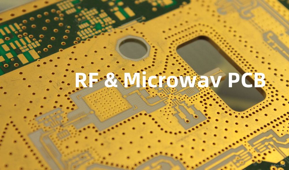
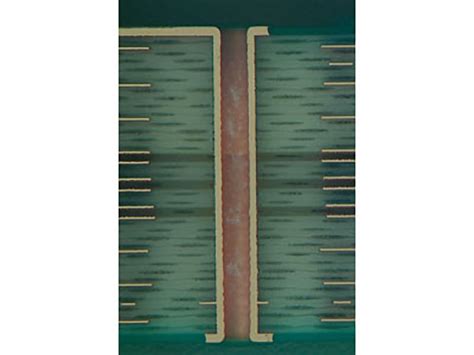
Multilayer PCBs, also known as multilayer printed circuit boards, are advanced circuit boards that consist of multiple layers of conductive material separated by insulating layers. These PCBs are designed to accommodate complex electronic circuits and provide a higher level of functionality and performance compared to single or double-layer PCBs.
The Structure of Multilayer PCBs
A typical multilayer PCB is composed of the following layers:
-
Copper layers: These are the conductive layers that carry electrical signals and power throughout the PCB. The number of copper layers can vary depending on the complexity of the circuit and the required performance.
-
Insulating layers: These layers, made of materials such as FR-4 or polyimide, separate the copper layers and prevent short circuits. They also provide mechanical support to the PCB.
-
Solder mask: This layer is applied on top of the outer copper layers to protect them from oxidation and prevent solder bridges during the assembly process.
-
Silkscreen: This layer is used to print text, logos, and component designators on the surface of the PCB for easy identification during assembly and troubleshooting.
| Layer | Material | Function |
|---|---|---|
| Copper | Copper | Carries electrical signals and power |
| Insulating | FR-4, Polyimide | Separates copper layers and provides mechanical support |
| Solder Mask | Polymer | Protects copper layers from oxidation and solder bridges |
| Silkscreen | Ink | Prints text, logos, and component designators |
Advantages of Multilayer PCBs
Increased Circuit Density
One of the primary advantages of multilayer PCBs is their ability to accommodate a higher number of components and more complex circuits in a smaller space. By utilizing multiple layers, designers can route traces more efficiently and reduce the overall size of the PCB.
Improved Signal Integrity
Multilayer PCBs offer better signal integrity compared to single or double-layer boards. The use of dedicated ground and power planes helps to reduce electromagnetic interference (EMI) and crosstalk between signals. This is particularly important for high-speed digital circuits and sensitive analog circuits.
Enhanced Thermal Management
The increased number of copper layers in a multilayer PCB provides better thermal conductivity, allowing heat to dissipate more efficiently from components. This helps to prevent overheating and improves the overall reliability of the electronic device.
Greater Mechanical Strength
The additional layers in a multilayer PCB contribute to its mechanical strength, making it more resistant to vibrations and physical stress. This is particularly beneficial for applications that require rugged and durable electronic assemblies.
Applications of Multilayer PCBs
Multilayer PCBs find applications in a wide range of industries, including:
- Consumer electronics: Smartphones, tablets, laptops, and wearables.
- Automotive: Engine control units, infotainment systems, and advanced driver assistance systems (ADAS).
- Medical devices: Diagnostic equipment, monitoring systems, and implantable devices.
- Aerospace and defense: Avionics, radar systems, and military communication equipment.
- Industrial automation: Programmable logic controllers (PLCs), human-machine interfaces (HMIs), and robotics.

Designing Multilayer PCBs
Layer Stackup
The layer stackup is a crucial aspect of multilayer PCB design. It defines the arrangement of copper and insulating layers, as well as their thicknesses. A well-designed stackup ensures proper signal integrity, impedance control, and manufacturability.
Signal Routing
When routing signals on a multilayer PCB, designers must consider factors such as trace width, spacing, and impedance. Proper signal routing techniques, such as the use of vias and controlled impedance traces, help to maintain signal integrity and prevent issues like crosstalk and reflections.
Power and Ground Distribution
Effective power and ground distribution is essential for the proper functioning of a multilayer PCB. Dedicated power and ground planes provide low-impedance paths for current flow and help to reduce noise and voltage drops. Designers must also consider the placement of decoupling capacitors to minimize high-frequency noise.
Thermal Management
Thermal management is an important consideration in multilayer PCB design. Proper placement of components and the use of thermal vias can help to dissipate heat more efficiently. In some cases, designers may also incorporate dedicated thermal layers or use high-thermal-conductivity materials to improve heat transfer.
Manufacturing Multilayer PCBs
Fabrication Process
The manufacturing of multilayer PCBs involves several steps:
- Inner layer processing: The inner copper layers are patterned and etched according to the design.
- Lamination: The inner layers are laminated together with insulating material under high temperature and pressure.
- Drilling: Holes are drilled through the laminated board for vias and component mounting.
- Plating: The drilled holes are plated with copper to create electrical connections between layers.
- Outer layer processing: The outer copper layers are patterned and etched.
- Solder mask and silkscreen application: The solder mask and silkscreen layers are applied to the outer surfaces of the PCB.
Quality Control
Strict quality control measures are essential during the manufacturing of multilayer PCBs. These measures include:
- Automated optical inspection (AOI): Used to detect surface defects, such as shorts, opens, and misaligned components.
- X-ray inspection: Employed to inspect the internal structure of the PCB, including vias and buried components.
- Electrical testing: Performed to verify the continuity and isolation of electrical connections, as well as to ensure the proper functioning of the circuit.
Future Trends in Multilayer PCBs
High-Density Interconnect (HDI) PCBs
HDI PCBs are a type of multilayer PCB that feature finer trace widths and spacings, smaller vias, and higher layer counts. These boards are designed to accommodate the ever-increasing demand for miniaturization and high-performance electronics.
Embedded Components
Embedded components, such as resistors, capacitors, and even active devices, are becoming more common in multilayer PCBs. By embedding these components within the layers of the PCB, designers can achieve higher circuit density and improved performance.
Advanced Materials
The development of advanced materials, such as low-loss dielectrics and high-thermal-conductivity substrates, is enabling the design of multilayer PCBs for high-frequency and high-power applications. These materials help to minimize signal loss, improve thermal management, and enhance the overall performance of the electronic device.
Frequently Asked Questions (FAQ)
-
Q: What is the difference between a multilayer PCB and a Single-Layer PCB?
A: A multilayer PCB consists of three or more conductive layers separated by insulating layers, while a single-layer PCB has only one conductive layer. Multilayer PCBs offer higher circuit density, better signal integrity, and improved thermal management compared to single-layer PCBs. -
Q: How many layers can a multilayer PCB have?
A: The number of layers in a multilayer PCB can vary depending on the complexity of the circuit and the application requirements. Common layer counts include 4, 6, 8, and 10 layers, but some advanced PCBs can have up to 50 layers or more. -
Q: What materials are used for the insulating layers in a multilayer PCB?
A: The most common materials used for the insulating layers in a multilayer PCB are FR-4 and polyimide. FR-4 is a glass-reinforced epoxy laminate that offers good mechanical and electrical properties, while polyimide is a high-performance material that can withstand higher temperatures and has better electrical characteristics. -
Q: What are the advantages of using dedicated ground and power planes in a multilayer PCB?
A: Dedicated ground and power planes in a multilayer PCB provide low-impedance paths for current flow, which helps to reduce electromagnetic interference (EMI) and crosstalk between signals. They also contribute to better thermal management by allowing heat to dissipate more efficiently from components. -
Q: What are the challenges in manufacturing multilayer PCBs?
A: The main challenges in manufacturing multilayer PCBs include ensuring proper alignment of layers during lamination, maintaining consistent dielectric thickness, and achieving reliable plating of vias and through-holes. Strict quality control measures, such as automated optical inspection (AOI) and X-ray inspection, are essential to identify and correct any defects during the manufacturing process.
In conclusion, multilayer PCBs are essential components in modern electronics, offering higher circuit density, improved signal integrity, and better thermal management compared to single or double-layer PCBs. By understanding the structure, advantages, and design considerations of multilayer PCBs, engineers can create more efficient and reliable electronic devices for a wide range of applications.

No responses yet