What are PCB stencils?
PCB Stencils, also known as solder paste stencils, are thin metal sheets with precise cutouts that correspond to the pads on a printed circuit board (PCB). These stencils are used to apply solder paste onto the PCB pads during the surface mount technology (SMT) assembly process. The solder paste is a mixture of tiny solder particles suspended in a flux medium, which helps to create a strong electrical and mechanical connection between the components and the PCB.
How are PCB Stencils Made?
PCB stencils are typically made from stainless steel, brass, or nickel. The stencil fabrication process involves several steps:
- Design: The stencil design is created based on the PCB Layout, taking into account the pad sizes, shapes, and pitch.
- Cutting: The stencil is cut using either laser cutting or chemical etching. Laser cutting is more precise and faster, while chemical etching is more cost-effective for larger quantities.
- Finishing: The stencil undergoes a cleaning and polishing process to remove any burrs or rough edges.
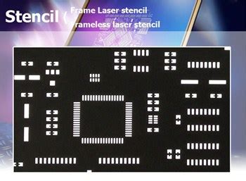
Types of PCB Stencils
There are several types of PCB stencils, each with its own characteristics and applications:
1. Stainless Steel Stencils
Stainless steel stencils are the most common type of PCB stencils. They are durable, long-lasting, and suitable for high-volume production. Stainless steel stencils are available in various thicknesses, typically ranging from 0.1 mm to 0.2 mm (4-8 mils).
2. Brass Stencils
Brass stencils are less expensive than stainless steel stencils and are suitable for prototyping and low-volume production. However, they are less durable and more prone to wear and tear.
3. Nickel Stencils
Nickel stencils are known for their excellent durability and corrosion resistance. They are more expensive than stainless steel and brass stencils but offer superior performance in harsh environments.
4. Framed Stencils
Framed stencils have a metal frame around the perimeter of the stencil, which provides additional stability and rigidity. This is particularly useful for larger PCBs or when using thinner stencils.
5. Stepped Stencils
Stepped stencils have different thicknesses for different areas of the PCB. This allows for better control over the solder paste deposition, especially when dealing with components of varying sizes or fine-pitch devices.

Using PCB Stencils
The process of using PCB stencils involves several steps:
- Alignment: The stencil is aligned with the PCB using fiducial marks or alignment pins to ensure accurate solder paste deposition.
- Solder Paste Application: Solder paste is applied onto the stencil using a squeegee or automated dispensing equipment. The squeegee is moved across the stencil, forcing the solder paste through the openings and onto the PCB pads.
- Stencil Removal: The stencil is carefully lifted away from the PCB, leaving the solder paste deposits on the pads.
- Component Placement: The surface mount components are placed onto the solder paste deposits using pick-and-place machines or manual placement.
- Reflow Soldering: The PCB undergoes a reflow soldering process, where the solder paste is heated to its melting point, creating a strong bond between the components and the PCB.

Costs of PCB Stencils
The cost of PCB stencils varies depending on several factors, such as the stencil material, size, thickness, and quantity. Here is a rough estimate of the costs for different stencil types:
| Stencil Type | Thickness (mm) | Price Range (USD) |
|---|---|---|
| Stainless Steel | 0.1 – 0.2 | $100 – $300 |
| Brass | 0.1 – 0.2 | $80 – $250 |
| Nickel | 0.1 – 0.2 | $150 – $400 |
| Framed Stencil | 0.1 – 0.2 | $200 – $500 |
| Stepped Stencil | 0.1 – 0.2 | $200 – $600 |
Note that these prices are for reference only and may vary depending on the supplier, location, and specific requirements.

Frequently Asked Questions (FAQ)
1. What is the recommended stencil thickness for my PCB?
The recommended stencil thickness depends on the size and pitch of the components on your PCB. As a general guideline:
- For standard SMD components (0603, 0805, etc.): 0.1 mm – 0.15 mm (4-6 mils)
- For fine-pitch components (0402, 0201, etc.): 0.08 mm – 0.1 mm (3-4 mils)
- For larger components or connectors: 0.15 mm – 0.2 mm (6-8 mils)
2. How long do PCB stencils last?
The lifespan of a PCB stencil depends on the material, usage, and maintenance. Stainless steel stencils can last for thousands of prints with proper care, while brass stencils have a shorter lifespan due to their lower durability.
3. Can I reuse a PCB stencil?
Yes, PCB stencils can be reused multiple times. However, it is essential to clean the stencil thoroughly after each use to remove any residual solder paste and prevent clogging of the apertures.
4. How do I store PCB stencils when not in use?
PCB stencils should be stored in a clean, dry environment to prevent corrosion and damage. It is recommended to store them in a protective case or sleeve and avoid stacking heavy objects on top of them.
5. Can I make my own PCB stencils?
While it is possible to make PCB stencils in-house using laser cutting or chemical etching equipment, it is generally more cost-effective and time-efficient to outsource stencil fabrication to specialized suppliers, especially for high-volume production.
Conclusion
PCB stencils are essential tools in the SMT Assembly process, enabling precise and consistent solder paste deposition on PCB pads. Choosing the right type of stencil and maintaining it properly can significantly improve the quality and reliability of the assembled PCBs. By understanding the types, uses, and costs of PCB stencils, electronics manufacturers can optimize their assembly processes and achieve better results.
No responses yet