Introduction to PCB Prototyping
Printed Circuit Board (PCB) prototyping is a crucial step in the development of electronic devices. It allows designers and engineers to test and validate their designs before committing to full-scale production. PCB prototypes are used to verify the functionality, reliability, and manufacturability of the designed circuit. In this article, we will explore the PCB prototype manufacturing process in detail.
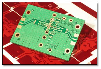
What is a PCB Prototype?
A PCB prototype is a preliminary version of a printed circuit board that is used for testing and validation purposes. It is a physical realization of the designed circuit, created using various manufacturing techniques. PCB prototypes are essential for identifying and resolving any issues or defects in the design before mass production.
Importance of PCB Prototyping
PCB prototyping plays a vital role in the electronics industry for several reasons:
-
Design Verification: Prototypes allow designers to test the functionality and performance of their circuits in real-world conditions. They can identify any design flaws, such as signal integrity issues or component compatibility problems, and make necessary revisions.
-
Cost Savings: By identifying and resolving issues during the prototyping stage, companies can avoid costly mistakes and rework during mass production. Prototyping helps minimize the risk of producing faulty or non-functional boards in large quantities.
-
Time-to-Market: PCB prototyping enables faster iterations and refinements of the design. It allows for quick testing and validation, reducing the overall development time and accelerating the time-to-market for the final product.
-
Manufacturability Assessment: Prototypes help assess the manufacturability of the designed circuit. They can reveal any challenges or limitations in the manufacturing process, allowing for design optimizations to improve production efficiency and yield.
PCB Prototype Manufacturing Process
The PCB prototype manufacturing process involves several key steps, from design creation to the final assembly of the prototype board. Let’s explore each step in detail.
Step 1: Design Creation
The first step in PCB prototyping is creating the circuit design using specialized software tools. Designers use Electronic Design Automation (EDA) software to create schematic diagrams and layout the components on the board. The design files typically include:
- Schematic diagram: A graphical representation of the circuit’s components and their interconnections.
- Bill of Materials (BOM): A list of all the components required for the circuit, including their part numbers, quantities, and specifications.
- PCB layout: The physical arrangement of components and traces on the board, considering factors such as component placement, routing, and signal integrity.
Step 2: Design Review and Verification
Once the initial design is created, it undergoes a thorough review and verification process. This step involves:
-
Design Rule Check (DRC): The design is checked against a set of predefined rules to ensure compliance with manufacturing constraints and guidelines. DRC helps identify any design violations, such as insufficient clearances or trace widths.
-
Electrical Rule Check (ERC): The schematic is analyzed to verify the electrical connectivity and integrity of the circuit. ERC checks for issues like short circuits, open circuits, or incorrect pin assignments.
-
Simulation: The circuit design may be simulated using specialized software to predict its behavior and performance. Simulation helps identify potential issues and allows for design optimizations before physical prototyping.
Step 3: Gerber File Generation
After the design is reviewed and verified, the next step is to generate Gerber files. Gerber files are industry-standard file formats used to describe the PCB layout for manufacturing. They contain information about the copper layers, solder mask, silkscreen, and drill holes. The commonly used Gerber file formats include:
| File Extension | Description |
|---|---|
| .GTL | Top copper layer |
| .GBL | Bottom copper layer |
| .GTO | Top silkscreen layer |
| .GBO | Bottom silkscreen layer |
| .GTS | Top solder mask layer |
| .GBS | Bottom solder mask layer |
| .TXT or .DRL | Drill file |
Step 4: PCB Fabrication
With the Gerber files ready, the next step is to fabricate the PCB prototype. The fabrication process involves several sub-steps:
-
Copper Etching: The PCB substrate, typically made of FR-4 material, is coated with a thin layer of copper. The unwanted copper areas are etched away using a chemical process, leaving behind the desired copper traces and pads as per the Gerber files.
-
Drilling: Holes are drilled into the PCB substrate at specific locations to accommodate through-hole components and vias. The drill file provides the necessary information for the drilling process.
-
Solder Mask Application: A solder mask layer is applied to the PCB surface to protect the copper traces from oxidation and prevent solder bridges during the assembly process. The solder mask is typically green in color but can be customized based on requirements.
-
Silkscreen Printing: The silkscreen layer is printed onto the PCB surface to add labels, logos, and component identifiers. This layer helps in the assembly process and provides visual reference for the board.
-
Surface Finish: A surface finish, such as Immersion Gold (ENIG), Immersion Silver (IAg), or Hot Air Solder Leveling (HASL), is applied to the exposed copper pads to protect them from oxidation and enhance solderability.
Step 5: PCB Assembly
Once the PCB is fabricated, the next step is to assemble the components onto the board. The assembly process can be done manually or using automated equipment, depending on the complexity and quantity of the prototypes. The assembly process involves:
-
Solder Paste Application: Solder paste, a mixture of tiny solder particles and flux, is applied to the pads on the PCB using a stencil or syringe. The solder paste helps in the attachment of surface-mount components.
-
Component Placement: The components are placed onto the PCB at their designated locations. For surface-mount components, the leads are aligned with the solder paste. Through-hole components are inserted into the drilled holes.
-
Reflow Soldering: The PCB with the placed components is subjected to a controlled heating process called reflow soldering. The solder paste melts and forms a strong mechanical and electrical bond between the components and the PCB pads.
-
Inspection: After the soldering process, the assembled PCB undergoes visual inspection to check for any defects, such as solder bridges, component misalignment, or poor solder joints. Automated optical inspection (AOI) systems may be used for more precise and efficient inspection.
Step 6: Testing and Validation
The assembled PCB prototype is then subjected to various testing and validation procedures to ensure its functionality and reliability. Common testing methods include:
-
Power-On Test: The prototype is powered on to verify that it turns on and functions as intended without any immediate issues.
-
Functional Test: The prototype is tested against its specified functional requirements to ensure that it performs as expected. This may involve testing individual components, subsystems, or the entire board.
-
In-Circuit Test (ICT): An automated test system is used to verify the integrity of the PCB assembly by checking for short circuits, open circuits, and component values.
-
Boundary Scan Test: For complex boards with high component density, boundary scan testing is used to test the interconnections and functionality of the components using a standard test access port (TAP).
-
Environmental Testing: Depending on the intended application, the prototype may be subjected to environmental tests such as temperature cycling, humidity exposure, or vibration testing to assess its durability and reliability.

PCB Prototype Manufacturing Techniques
There are several manufacturing techniques used for PCB prototyping, each with its own advantages and limitations. Let’s explore some of the common techniques:
1. Traditional Etching
Traditional etching is the most widely used method for PCB prototyping. It involves the following steps:
- The PCB design is printed onto a transparent film called a photomask.
- The copper-clad PCB substrate is coated with a light-sensitive photoresist material.
- The photomask is placed on top of the photoresist, and the board is exposed to UV light. The areas exposed to light become soluble in a developer solution.
- The board is developed, removing the soluble photoresist and exposing the underlying copper.
- The exposed copper is etched away using a chemical solution, leaving behind the desired copper traces and pads.
Traditional etching offers good accuracy and is suitable for most standard PCB designs. However, it has limitations in terms of minimum feature sizes and requires the use of chemicals.
2. CNC Milling
CNC (Computer Numerical Control) milling is a subtractive manufacturing technique used for PCB prototyping. It involves the following steps:
- The PCB design is converted into a set of machine-readable instructions called G-code.
- A CNC milling machine, equipped with a high-speed spindle and precise motion control, is used to mill away the unwanted copper from the PCB substrate.
- The milling tool follows the G-code instructions to create the desired copper traces and pads on the board.
CNC milling offers several advantages, such as quick turnaround times, the ability to create complex shapes, and the elimination of chemicals. However, it has limitations in terms of minimum feature sizes and may not be suitable for high-density designs.
3. 3D Printing
3D printing is an additive manufacturing technique that is gaining popularity for PCB prototyping. It involves the following steps:
- The PCB design is converted into a 3D model, including the substrate, copper traces, and components.
- A 3D printer, typically using Fused Deposition Modeling (FDM) technology, is used to print the PCB layer by layer.
- Conductive ink or filament is used to print the copper traces and pads.
- The components are manually placed and soldered onto the printed PCB.
3D printing offers rapid prototyping capabilities and allows for the creation of complex 3D structures. However, the resolution and conductivity of the printed traces may not match those of traditional PCB manufacturing methods.
4. Laser Direct Imaging (LDI)
Laser Direct Imaging (LDI) is a high-precision PCB prototyping technique that uses a laser to directly expose the photoresist on the PCB substrate. It involves the following steps:
- The PCB design is loaded into the LDI system’s software.
- The copper-clad PCB substrate is coated with a photoresist material.
- A high-resolution laser beam directly exposes the photoresist according to the PCB design.
- The exposed photoresist is developed, and the unexposed areas are removed.
- The exposed copper is etched away, leaving behind the desired copper traces and pads.
LDI offers high accuracy and resolution, enabling the creation of fine pitch and high-density PCB designs. It eliminates the need for photomasks and offers quick turnaround times.

Advantages of PCB Prototyping
PCB prototyping offers several advantages in the electronics design and development process:
-
Early Design Validation: Prototyping allows designers to validate their circuit designs early in the development cycle. They can test the functionality, performance, and reliability of the circuit under real-world conditions and make necessary modifications before committing to full-scale production.
-
Cost Savings: By identifying and resolving design issues during the prototyping stage, companies can avoid costly mistakes and rework during mass production. Prototyping helps minimize the risk of producing faulty or non-functional boards in large quantities, saving significant costs in the long run.
-
Faster Time-to-Market: PCB prototyping enables faster iterations and refinements of the design. Designers can quickly test and validate their designs, make necessary changes, and move to the next stage of development. This iterative process helps reduce the overall development time and accelerates the time-to-market for the final product.
-
Design Optimization: Prototyping provides an opportunity to optimize the PCB design for manufacturability, reliability, and performance. Designers can experiment with different component placements, routing strategies, and manufacturing techniques to improve the overall quality and efficiency of the final product.
-
Risk Mitigation: PCB prototyping helps mitigate risks associated with the development and production of electronic products. By thoroughly testing and validating the design through prototypes, companies can identify and address potential issues early on, reducing the likelihood of costly failures or recalls in the future.

Challenges in PCB Prototyping
While PCB prototyping offers numerous benefits, there are also some challenges that designers and manufacturers may face:
-
Cost: Prototyping can be expensive, especially for complex designs or high-density boards. The cost of materials, fabrication, assembly, and testing can add up quickly. Companies need to balance the benefits of prototyping with the associated costs and allocate resources accordingly.
-
Time Constraints: In fast-paced industries, time-to-market is crucial. PCB prototyping can be time-consuming, especially if multiple iterations are required. Designers need to efficiently manage the prototyping process, prioritize critical aspects of the design, and streamline the feedback and revision cycles to meet tight deadlines.
-
Design Complexity: As electronic devices become more sophisticated and compact, PCB designs are becoming increasingly complex. High-density boards, fine-pitch components, and advanced packaging technologies pose challenges for prototyping. Designers need to have a deep understanding of PCB design principles, manufacturing constraints, and signal integrity considerations to create reliable and manufacturable prototypes.
-
Component Availability: Prototyping often requires specific components that may have limited availability or long lead times. Designers need to carefully plan their component selections, considering factors such as availability, cost, and lead times. They may need to find alternative components or work closely with suppliers to ensure timely delivery of critical components for prototyping.
-
Manufacturing Limitations: Different PCB prototyping techniques have their own limitations in terms of minimum feature sizes, material compatibility, and manufacturing capabilities. Designers need to be aware of these limitations and design their boards accordingly. They may need to make trade-offs between design requirements and manufacturability to ensure successful prototyping.
Future Trends in PCB Prototyping
PCB prototyping technologies continue to evolve, driven by advancements in materials, manufacturing processes, and design tools. Some of the future trends in PCB prototyping include:
-
3D Printing: 3D printing technology is expected to play a larger role in PCB prototyping in the future. Advances in conductive materials, multi-material printing, and high-resolution printing techniques will enable the creation of more complex and functional 3D-printed PCBs. This will offer greater design flexibility and faster prototyping capabilities.
-
Advanced Materials: New materials, such as high-frequency laminates, flexible substrates, and embedded components, are being developed to meet the demands of emerging applications. These materials will enable the creation of PCB prototypes with improved performance, reliability, and functionality. Designers will have more options to choose from based on their specific requirements.
-
Intelligent Design Tools: PCB design software tools are becoming more intelligent and automated, leveraging artificial intelligence (AI) and machine learning algorithms. These tools will assist designers in optimizing PCB layouts, identifying potential issues, and suggesting design improvements. Intelligent design tools will help streamline the prototyping process and reduce the time and effort required for manual design tasks.
-
Virtual Prototyping: Virtual prototyping techniques, such as simulation and emulation, are gaining traction in the PCB design process. These techniques allow designers to virtually test and validate their designs before physical prototyping. Virtual prototyping helps identify and resolve issues early in the design cycle, reducing the need for multiple physical prototype iterations and saving time and costs.
-
Collaborative Prototyping: Cloud-based platforms and collaborative design tools are enabling better collaboration among PCB designers, manufacturers, and stakeholders. These platforms allow seamless sharing of design files, real-time feedback, and version control. Collaborative prototyping will facilitate faster iterations, improved communication, and streamlined workflows in the prototyping process.
Conclusion
PCB prototyping is a critical step in the development of electronic products, allowing designers to test, validate, and optimize their designs before mass production. The PCB prototype manufacturing process involves several key steps, including design creation, fabrication, assembly, and testing. Various manufacturing techniques, such as traditional etching, CNC milling, 3D printing, and laser direct imaging, are used for PCB prototyping, each with its own advantages and limitations.
PCB prototyping offers numerous benefits, including early design validation, cost savings, faster time-to-market, design optimization, and risk mitigation. However, it also presents challenges, such as cost, time constraints, design complexity, component availability, and manufacturing limitations.
As PCB technologies continue to evolve, future trends in PCB prototyping include advancements in 3D printing, advanced materials, intelligent design tools, virtual prototyping, and collaborative prototyping. These trends will shape the future of PCB design and manufacturing, enabling faster, more efficient, and more innovative prototyping processes.
Frequently Asked Questions (FAQ)
-
What is the purpose of PCB prototyping?
PCB prototyping is done to test and validate the functionality, performance, and manufacturability of a PCB design before committing to full-scale production. It helps identify and resolve any issues or defects in the design early in the development cycle. -
**How long does it take to manufacture
No responses yet