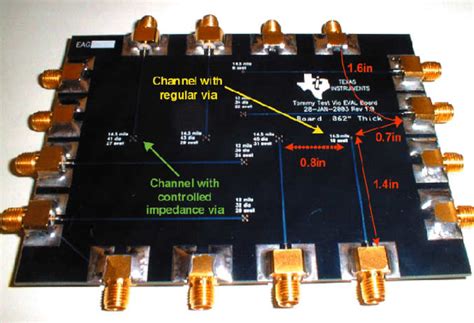
What is Controlled Impedance?
Controlled impedance refers to the precise management of impedance within an electrical circuit. Impedance is a measure of the total opposition that a circuit presents to alternating current (AC), taking into account resistance, capacitance, and inductance. In high-speed digital systems, it is crucial to control the impedance of transmission lines to ensure signal integrity and optimal performance.
Key Aspects of Controlled Impedance
- Characteristic Impedance (Z0)
- Determined by the physical properties of the transmission line (e.g., geometry, materials)
-
Typically designed to match the source and load impedances to minimize reflections
-
Impedance Matching
- Ensuring that the impedance of the source, transmission line, and load are closely matched
-
Minimizes signal reflections and power loss
-
Signal Integrity
- Maintaining the quality and fidelity of signals as they propagate through the system
- Reducing signal distortion, attenuation, and crosstalk
Why is Controlled Impedance Critical?
High-Speed Digital Systems
In modern high-speed digital systems, controlled impedance is essential for several reasons:
- Signal Integrity
- As data rates increase, signal rise and fall times become shorter
- Uncontrolled impedance can lead to signal reflections, causing distortion and reducing signal quality
-
Controlling impedance helps maintain signal integrity, ensuring reliable data transmission
-
Timing and Synchronization
- Impedance mismatches can cause signal delays and skew
-
Controlled impedance helps maintain consistent signal propagation delays, critical for proper timing and synchronization
-
Power Efficiency
- Impedance mismatches result in power being reflected back to the source
-
Controlled impedance minimizes reflections, reducing power loss and improving overall system efficiency
-
Electromagnetic Compatibility (EMC)
- Uncontrolled impedance can lead to electromagnetic interference (EMI) and compatibility issues
- Controlled impedance helps contain electromagnetic emissions, ensuring compliance with EMC regulations
Applications Requiring Controlled Impedance
Controlled impedance is crucial in various applications, including:
- High-speed digital interfaces (e.g., USB, PCIe, HDMI)
- Telecommunications and networking equipment
- Radar and wireless systems
- Aerospace and defense electronics
- Medical devices and imaging systems

Designing for Controlled Impedance
Factors Affecting Impedance
Several factors influence the impedance of a transmission line:
- Conductor geometry (width, thickness, spacing)
- Dielectric properties of the substrate material
- Trace routing and layout
- Manufacturing tolerances
Impedance Calculation and Simulation
To design for controlled impedance, engineers use various tools and techniques:
- Impedance Calculators
- Analytical tools that estimate impedance based on trace geometry and substrate properties
-
Provide a starting point for impedance-controlled designs
-
Electromagnetic simulation software
- Numerical modeling tools that accurately simulate the electromagnetic behavior of transmission lines
-
Help optimize trace geometry and spacing to achieve the desired impedance
-
Design rules and guidelines
- Industry-standard design rules for controlled impedance (e.g., IPC-2141, IPC-2251)
- Provide recommendations for trace geometry, spacing, and layer stackup
Impedance Control in PCB Manufacturing
To ensure consistent impedance in the final product, PCB manufacturers employ several techniques:
- Impedance testing
- Measuring the impedance of manufactured PCBs using time-domain reflectometry (TDR) or other methods
-
Verifying that the impedance meets the specified tolerance
-
Process control
- Monitoring and controlling the manufacturing process parameters that affect impedance (e.g., etching, lamination)
-
Implementing statistical process control (SPC) to maintain consistency
-
Material selection
- Choosing substrate materials with stable dielectric properties
- Using low-loss, high-performance materials for demanding applications

Challenges and Considerations
Manufacturing Tolerances
One of the main challenges in controlling impedance is dealing with manufacturing tolerances:
- Variation in conductor width and thickness
- Dielectric thickness and permittivity variations
- Alignment and registration errors
To account for these tolerances, designers typically specify an impedance tolerance (e.g., ±10%) and work closely with PCB manufacturers to ensure compliance.
Material Selection and Cost
Selecting the appropriate substrate material is crucial for achieving controlled impedance:
- High-performance materials (e.g., low-loss, tightly controlled dielectrics) offer better impedance control but at a higher cost
- Designers must balance performance requirements with cost constraints
- Hybrid stackups, combining standard and high-performance materials, can provide a cost-effective solution
Design Complexity and Density
As design complexity and density increase, controlling impedance becomes more challenging:
- Higher layer counts and smaller feature sizes make impedance control more difficult
- Increased crosstalk and electromagnetic coupling between traces
- Need for advanced design tools and simulation techniques to optimize impedance

FAQ
1. What is the difference between differential and single-ended impedance?
Differential impedance refers to the impedance of a pair of conductors with opposite polarity signals, while single-ended impedance refers to the impedance of a single conductor with respect to a reference plane (e.g., ground). Differential signaling is often used in high-speed applications due to its better noise immunity and reduced electromagnetic emissions.
2. How does the dielectric constant of a substrate material affect impedance?
The dielectric constant (εr) of a substrate material directly affects the impedance of a transmission line. A higher dielectric constant results in lower impedance, while a lower dielectric constant leads to higher impedance. The relationship between impedance and dielectric constant is given by:
Z0 = (87 / √εr) * ln(5.98 * h / (0.8 * w + t))
where:
– Z0 is the characteristic impedance
– εr is the dielectric constant
– h is the dielectric thickness
– w is the trace width
– t is the trace thickness
3. What is the typical impedance tolerance for controlled impedance PCBs?
The typical impedance tolerance for controlled impedance PCBs is ±10%. This means that the actual impedance of the manufactured PCB should be within ±10% of the specified target impedance. Tighter tolerances (e.g., ±5%) are possible but may increase manufacturing costs and complexity.
4. Can controlled impedance be achieved on a standard FR-4 substrate?
Yes, controlled impedance can be achieved on a standard FR-4 substrate, although with some limitations. FR-4 has a relatively high dielectric constant (εr ≈ 4.3) and a dissipation factor that increases with frequency, which can lead to higher losses and signal attenuation at high frequencies. For demanding high-speed applications, low-loss materials with tightly controlled dielectric properties (e.g., Rogers RO4000 series) may be preferred.
5. What is the role of a time-domain reflectometer (TDR) in controlled impedance testing?
A time-domain reflectometer (TDR) is an instrument used to measure the impedance of a transmission line by sending a fast-rising pulse down the line and analyzing the reflected signal. TDR measurements provide a detailed view of the impedance profile along the length of the line, allowing engineers to identify impedance discontinuities, mismatches, and other anomalies. TDR is widely used in PCB manufacturing for impedance testing and Quality Control.
Conclusion
Controlled impedance is a critical aspect of modern high-speed digital design, ensuring signal integrity, reliable data transmission, and optimal system performance. By carefully designing transmission lines, selecting appropriate materials, and working closely with PCB manufacturers, engineers can achieve controlled impedance and meet the demanding requirements of today’s advanced electronic systems. As data rates continue to increase and designs become more complex, the importance of controlled impedance will only continue to grow, driving innovation in design tools, manufacturing processes, and materials science.
| Aspect | Importance |
|---|---|
| Signal Integrity | Maintains signal quality and fidelity, ensuring reliable data transmission |
| Timing & Synchronization | Ensures consistent signal propagation delays for proper timing |
| Power Efficiency | Minimizes reflections and power loss, improving overall system efficiency |
| EMC Compliance | Helps contain electromagnetic emissions, ensuring compliance with regulations |
Table 1: Key aspects of controlled impedance and their importance in high-speed digital systems.
| Material | Dielectric Constant (εr) | Dissipation Factor (Df) | Typical Applications |
|---|---|---|---|
| FR-4 | 4.3 – 4.6 | 0.02 – 0.03 | General-purpose PCBs |
| Rogers RO4003C | 3.38 | 0.0027 | High-frequency, low-loss applications |
| Isola I-Tera MT40 | 3.45 – 3.60 | 0.0030 – 0.0038 | High-speed digital, automotive radar |
| Nelco N4000-13SI | 3.70 | 0.0040 | High-speed digital, aerospace/defense |
Table 2: Common PCB Substrate Materials and their properties for controlled impedance applications.
No responses yet