Introduction to PCBs
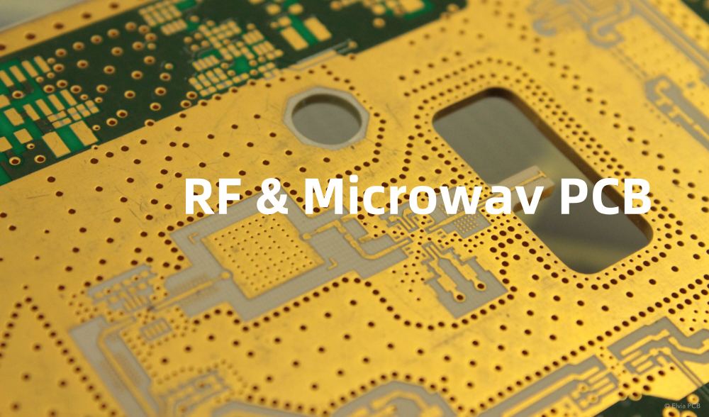
A printed circuit board (PCB) is a fundamental component in modern electronics. It is a flat board made of insulating material, such as fiberglass, with conductive copper traces printed on its surface. These traces connect various electronic components, such as resistors, capacitors, and integrated circuits, to form a complete circuit. PCBs are used in almost all electronic devices, from simple gadgets like calculators to complex systems like computers and smartphones.
In this comprehensive guide, we will walk you through the process of designing and fabricating your own PCB, from concept to finished product. Whether you’re a hobbyist, student, or professional, this guide will provide you with the knowledge and skills necessary to create your own custom PCBs.
Understanding PCB Basics
PCB Layers
PCBs can be classified based on the number of conductive layers they have:
| PCB Type | Number of Layers |
|---|---|
| Single-sided | 1 |
| Double-sided | 2 |
| Multi-layer | 4, 6, 8, or more |
Single-Sided PCBs have conductive traces on only one side of the board, while double-sided PCBs have traces on both sides. Multi-layer PCBs have additional layers of conductive material sandwiched between insulating layers, allowing for more complex circuit designs and higher component density.
PCB Materials
The most common materials used for PCB substrates are:
- FR-4: A flame-retardant fiberglass-reinforced epoxy laminate, widely used for its good electrical insulation properties and mechanical strength.
- Polyimide: A high-temperature resistant material used in applications that require greater thermal stability.
- Aluminum: Used for PCBs that require better heat dissipation, such as high-power LED boards or motor controllers.
The choice of material depends on the specific requirements of your project, such as operating temperature, mechanical stress, and electrical properties.
Designing Your PCB
Schematic Design
The first step in creating a PCB is to design the schematic diagram of your circuit. A schematic is a graphical representation of the electrical connections between components. It uses standardized symbols to represent components and lines to represent the connections between them.
To create a schematic, you can use various electronic design automation (EDA) software, such as:
- KiCad
- Eagle
- Altium Designer
- OrCAD
These software packages offer schematic capture tools that allow you to place components and draw connections easily. They also provide libraries of common components, which you can use to quickly build your circuit.
PCB Layout
Once you have completed the schematic design, the next step is to create the PCB layout. The layout is a physical representation of your circuit, showing the actual size and position of components and traces on the board.
To create a PCB layout, you will use the same EDA software used for schematic design. The software will import the schematic and allow you to place components and route traces between them. When designing the layout, consider the following factors:
- Component placement: Arrange components in a logical manner, minimizing the distance between connected components to reduce trace length and improve signal integrity.
- Trace width: Choose appropriate trace widths based on the current carrying requirements of your circuit. Wider traces can handle higher currents but occupy more space on the board.
- Clearance: Ensure adequate clearance between traces and components to avoid short circuits and manufacturing issues.
- Ground planes: Use ground planes to provide a low-impedance return path for signals and to reduce electromagnetic interference (EMI).

Manufacturing Your PCB
PCB Fabrication Methods
There are several methods for fabricating PCBs, each with its own advantages and limitations:
- Etching: This is the most common method for hobbyists and small-scale production. It involves transferring the PCB layout onto a copper-clad board using a photoresist process and then etching away the unwanted copper using a chemical solution.
- Milling: A CNC machine is used to mill away the unwanted copper, leaving behind the desired traces. This method is suitable for prototyping and low-volume production.
- Professional fabrication: For high-volume production or complex designs, it is best to use a professional PCB fabrication service. These services use advanced manufacturing techniques, such as photolithography and electroplating, to produce high-quality PCBs.
PCB Assembly
After fabricating the PCB, the next step is to assemble the components onto the board. There are two main methods for PCB assembly:
- Through-hole: Components with long leads are inserted through holes drilled in the PCB and soldered on the opposite side. This method is easier for manual assembly but requires more space on the board.
- Surface-mount: Components are placed directly on the surface of the PCB and soldered in place. This method allows for higher component density but requires more precise placement and soldering techniques.
You can assemble your PCB manually using a soldering iron and tweezers, or you can use a pick-and-place machine for automated assembly.
Testing and Troubleshooting
After assembling your PCB, it is essential to test it thoroughly to ensure proper functionality. Here are some tips for testing and troubleshooting your PCB:
- Visual inspection: Carefully inspect the PCB for any visible defects, such as short circuits, cold solder joints, or damaged components.
- Continuity testing: Use a multimeter to test for continuity between connected points on the PCB. This will help you identify any open circuits or broken traces.
- Power-on testing: Apply power to the PCB and check for the expected voltages at various points in the circuit. If the voltages are incorrect, it may indicate a problem with the power supply or voltage regulation.
- Functional testing: Test the PCB’s functionality by applying the appropriate inputs and measuring the outputs. Compare the results with the expected behavior based on your circuit design.
If you encounter any issues during testing, use the following troubleshooting techniques:
- Check the schematic: Verify that the PCB layout matches the schematic design. Look for any discrepancies or errors in the connections.
- Check component values: Ensure that the correct component values are used and that they are placed in the right positions on the board.
- Check soldering: Inspect the solder joints for any cold or bridged connections. Reflow the solder if necessary.
- Use an oscilloscope: For more advanced troubleshooting, use an oscilloscope to analyze signals and identify any timing or noise issues.
Frequently Asked Questions (FAQ)
-
Q: What is the difference between a single-sided and double-sided PCB?
A: A single-sided PCB has conductive traces on only one side of the board, while a double-sided PCB has traces on both sides. Double-sided PCBs allow for more complex circuit designs and higher component density. -
Q: Can I design a PCB without using EDA software?
A: While it is possible to design a simple PCB by hand, using EDA software is highly recommended. EDA software provides tools for schematic capture, PCB layout, and design rule checking, which greatly simplify the design process and help avoid errors. -
Q: What is the best method for fabricating a PCB at home?
A: For hobbyists and small-scale production, etching is the most common method for fabricating PCBs at home. It involves transferring the PCB layout onto a copper-clad board using a photoresist process and then etching away the unwanted copper using a chemical solution. -
Q: How do I choose the appropriate trace width for my PCB?
A: The appropriate trace width depends on the current carrying requirements of your circuit. Wider traces can handle higher currents but occupy more space on the board. You can use online trace width calculators or refer to the IPC-2221 standard for guidance on choosing trace widths based on your specific requirements. -
Q: What should I do if my PCB is not functioning as expected?
A: If your PCB is not functioning as expected, start by performing a visual inspection for any visible defects. Then, use a multimeter to test for continuity and check for the expected voltages at various points in the circuit. If you still cannot identify the problem, use an oscilloscope to analyze signals and identify any timing or noise issues. Double-check your schematic and component values, and inspect the solder joints for any cold or bridged connections.
Conclusion
Designing and fabricating your own PCB can be a rewarding and educational experience. By understanding the basics of PCB Design, using the right tools and techniques, and following best practices for manufacturing and testing, you can create custom PCBs for your projects.
Remember to start with a clear schematic design, carefully plan your PCB layout, and choose the appropriate fabrication method based on your needs. When assembling your PCB, pay attention to component placement and soldering techniques to ensure a reliable and functional board.
If you encounter any issues during the design or fabrication process, don’t hesitate to seek help from online communities, tutorials, or experienced professionals. With practice and persistence, you’ll soon be creating complex and innovative PCBs for your electronic projects.

No responses yet