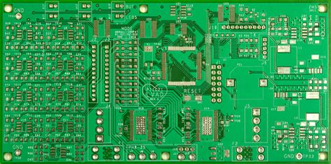
Introduction to PCB Layers
Printed Circuit Boards (PCBs) are the backbone of modern electronics. They provide a platform for mounting and interconnecting electronic components to create a functional circuit. One of the key decisions in PCB Design is choosing the appropriate number of layers. The most common options are 2 layer PCBs and 4 layer PCBs. In this article, we will explore the factors to consider when deciding between a 2 layer PCB and a 4 layer PCB.
What are PCB Layers?
PCB layers refer to the number of conductive copper layers that make up a printed circuit board. Each layer consists of a thin sheet of insulating material, typically fiberglass, with copper traces etched onto one or both sides. The layers are stacked and laminated together to form the complete PCB.
The most common PCB layer configurations are:
- Single-sided (1 layer): Copper traces on one side of the board
- Double-sided (2 layers): Copper traces on both sides of the board
- Multi-layer (4, 6, 8, or more layers): Multiple layers of copper traces separated by insulating material
Factors to Consider When Choosing Between 2 Layer and 4 Layer PCBs
1. Circuit Complexity
The complexity of your circuit is a primary factor in determining the number of layers required. Simple circuits with few components and interconnections can often be accommodated on a 2 layer PCB. However, as the circuit complexity increases, with more components and signal traces, a 4 layer PCB may become necessary.
Consider the following:
- Number of components: More components typically require more space and interconnections.
- Signal density: High signal density may require additional layers to avoid signal integrity issues.
- Routing complexity: Complex routing, such as dense ball grid array (BGA) packages, may necessitate additional layers.
2. Signal Integrity
Signal integrity refers to the quality of the electrical signals transmitted through the PCB. It is influenced by factors such as noise, crosstalk, and electromagnetic interference (EMI). In general, 4 layer PCBs offer better signal integrity than 2 layer PCBs.
Here’s how the number of layers affects signal integrity:
- Ground and power planes: 4 layer PCBs allow for dedicated ground and power planes, which provide a low-impedance return path for signals and help reduce noise.
- Signal separation: Additional layers in a 4 layer PCB allow for better separation between signal traces, reducing crosstalk.
- Shielding: The ground and power planes in a 4 layer PCB act as shields, helping to minimize EMI.
3. Power Distribution
Efficient power distribution is crucial for the proper functioning of electronic circuits. 4 layer PCBs have an advantage over 2 layer PCBs in terms of power distribution.
Consider the following:
- Power planes: 4 layer PCBs can have dedicated power planes, ensuring a low-impedance power distribution network.
- Voltage drop: The additional copper in a 4 layer PCB helps reduce voltage drop across the board, especially for high-current circuits.
- Decoupling: The proximity of power and ground planes in a 4 layer PCB improves decoupling performance, reducing noise on the Power Supply.
4. Cost and Manufacturing
The cost and manufacturing complexity are important considerations when choosing between a 2 layer and 4 layer PCB.
| Factor | 2 Layer PCB | 4 Layer PCB |
|---|---|---|
| Material Cost | Lower | Higher |
| Manufacturing Cost | Lower | Higher |
| Manufacturing Time | Shorter | Longer |
| Design Complexity | Simpler | More Complex |
In general, 2 layer PCBs are less expensive and faster to manufacture than 4 layer PCBs. However, the cost difference may be justified if the circuit complexity, signal integrity, or power distribution requirements demand a 4 layer PCB.
5. Board Size and Layer Stack-up
The size of your PCB and the layer stack-up can influence the decision between a 2 layer and 4 layer design.
- Board size: For smaller boards, a 2 layer PCB may suffice. As the board size increases, the benefits of a 4 layer PCB become more pronounced.
- Layer stack-up: The arrangement of layers in a 4 layer PCB can be optimized for signal integrity and power distribution. Common stack-ups include signal-ground-power-signal (S-G-P-S) and signal-ground-ground-signal (S-G-G-S).

When to Choose a 2 Layer PCB
A 2 layer PCB is a suitable choice under the following circumstances:
- Simple circuits with low component count and minimal interconnections.
- Low-speed digital circuits or analog circuits with relaxed signal integrity requirements.
- Projects with tight budget constraints, where cost is a primary concern.
- Prototypes or low-volume production runs, where the additional cost of a 4 layer PCB may not be justified.
- Circuits with ample board space, allowing for proper component placement and routing on two layers.

When to Choose a 4 Layer PCB
A 4 layer PCB is recommended in the following situations:
- Complex circuits with high component density and numerous interconnections.
- High-speed digital circuits or analog circuits with strict signal integrity requirements.
- Designs requiring efficient power distribution and low-impedance power delivery.
- Circuits susceptible to noise, crosstalk, or electromagnetic interference.
- Projects with space constraints, where the additional layers allow for more compact routing and component placement.

Frequently Asked Questions (FAQ)
1. Can I start with a 2 layer PCB and upgrade to a 4 layer PCB later?
While it is possible to redesign a 2 layer PCB into a 4 layer PCB, it is not a straightforward process. The additional layers will require changes to the component placement, routing, and layer stack-up. It is best to carefully consider your requirements upfront and choose the appropriate number of layers from the beginning.
2. Are there any disadvantages to using a 4 layer PCB?
The main disadvantages of a 4 layer PCB compared to a 2 layer PCB are the increased cost and longer manufacturing time. Additionally, designing a 4 layer PCB can be more complex, requiring careful consideration of signal integrity, power distribution, and layer stack-up.
3. Can I mix signal and power layers in a 4 layer PCB?
While it is possible to mix signal and power layers in a 4 layer PCB, it is generally not recommended. Dedicated signal and power layers provide better signal integrity and power distribution. Mixing them can lead to increased noise and crosstalk.
4. Are there any alternatives to 2 layer and 4 layer PCBs?
Yes, there are PCBs with more layers, such as 6, 8, or even more. These are typically used for highly complex circuits with strict signal integrity and power distribution requirements. There are also specialized PCBs, such as high-frequency PCBs and Flexible PCBs, which cater to specific applications.
5. How do I choose the right layer stack-up for my 4 layer PCB?
The choice of layer stack-up depends on your specific circuit requirements. Common stack-ups include signal-ground-power-signal (S-G-P-S) and signal-ground-ground-signal (S-G-G-S). Consult with your PCB manufacturer or an experienced PCB designer to determine the optimal layer stack-up for your application.
Conclusion
Choosing between a 2 layer PCB and a 4 layer PCB is a critical decision in PCB design. The number of layers directly impacts the circuit complexity, signal integrity, power distribution, cost, and manufacturing time. By carefully considering these factors and your specific project requirements, you can make an informed decision that balances performance, reliability, and cost.
In general, 2 layer PCBs are suitable for simple circuits with low component density and relaxed signal integrity requirements. They offer lower cost and faster manufacturing times. On the other hand, 4 layer PCBs are recommended for complex circuits with high component density, strict signal integrity requirements, and efficient power distribution needs. While they come at a higher cost and longer manufacturing time, the benefits they offer can be crucial for the success of your project.
Ultimately, the choice between a 2 layer PCB and a 4 layer PCB should be based on a thorough understanding of your circuit requirements, budget, and project goals. By making an informed decision and working closely with experienced PCB designers and manufacturers, you can ensure that your PCB meets your performance, reliability, and cost targets.
No responses yet