Introduction to PCB Solder Mask
PCB (Printed Circuit Board) solder mask is a protective layer applied to the copper traces of a PCB during the manufacturing process. Its primary purpose is to prevent solder bridges from forming between closely spaced solder pads, as well as to protect the copper traces from oxidation and contamination. Solder mask also provides electrical insulation, improves the circuit board’s appearance, and enhances the durability of the PCB.
What is a Solder Mask?
A solder mask, also known as a solder resist or solder stop mask, is a thin layer of polymer that is applied to the surface of a PCB. This layer is typically green in color but can also be found in other colors such as red, blue, black, or white. The solder mask covers the entire surface of the PCB except for the areas where components will be soldered, such as pads, through-holes, and vias.
The main functions of a solder mask are:
-
Preventing solder bridges: By covering the spaces between solder pads, the solder mask prevents solder from flowing and creating unintended connections (bridges) between adjacent pads.
-
Protecting copper traces: The solder mask shields the copper traces from oxidation, corrosion, and physical damage, which can occur during handling and assembly.
-
Providing electrical insulation: The solder mask acts as an insulating layer, preventing short circuits between copper traces and components.
-
Improving PCB appearance: Solder mask gives the PCB a clean, professional look and can be used to create text, logos, or other markings on the board’s surface.
-
Enhancing durability: The solder mask protects the PCB from moisture, dust, and other environmental factors that can degrade its performance over time.
Types of Solder Mask
There are two main types of solder mask used in PCB manufacturing:
- Liquid Photoimageable Solder Mask (LPSM):
- LPSM is the most common type of solder mask used in the PCB industry.
- It is applied as a liquid and then exposed to UV light through a photographic film, which hardens the exposed areas.
-
The unexposed areas are then removed using a developer solution, leaving the desired solder mask pattern on the PCB.
-
Dry Film Solder Mask (DFSM):
- DFSM is a solid film that is laminated onto the surface of the PCB using heat and pressure.
- It is then exposed to UV light through a photographic film, which polymerizes the exposed areas.
- The unexposed areas are removed using a developer solution, similar to the LPSM process.
| Property | Liquid Photoimageable Solder Mask (LPSM) | Dry Film Solder Mask (DFSM) |
|---|---|---|
| Application Method | Liquid coating | Dry film lamination |
| Exposure Method | UV light | UV light |
| Developing Process | Developer solution | Developer solution |
| Thickness Control | Adjustable by coating parameters | Fixed by film thickness |
| Resolution | High | Moderate |
| Adhesion to Copper | Good | Good |
| Mechanical Strength | Good | Excellent |
| Chemical Resistance | Good | Excellent |
| Cost | Lower | Higher |
| Suitability for Fine Pitch | Excellent | Good |
Solder Mask Application Process
The solder mask application process consists of several steps, which may vary slightly depending on the type of solder mask and the specific PCB Manufacturer’s processes. The general steps are as follows:
-
PCB Cleaning: The bare PCB is cleaned to remove any dirt, grease, or oxidation from the copper surface. This ensures proper adhesion of the solder mask.
-
Solder Mask Application: The solder mask is applied to the PCB surface using either the LPSM or DFSM method.
- For LPSM, the liquid solder mask is coated onto the PCB using a screen printing, curtain coating, or spraying process. The thickness of the coating is controlled by the application parameters.
-
For DFSM, the dry film is laminated onto the PCB surface using heat and pressure.
-
UV Exposure: The PCB with the applied solder mask is exposed to UV light through a photographic film (also called a solder mask film or phototool). The film contains the desired solder mask pattern, and the UV light polymerizes the exposed areas of the solder mask.
-
Developing: After exposure, the PCB is placed in a developer solution, which removes the unexposed areas of the solder mask. This step reveals the copper pads, through-holes, and vias that will be used for soldering components.
-
Curing: The PCB is then heated in an oven to fully cure the remaining solder mask. This process ensures that the mask achieves its final mechanical, chemical, and electrical properties.
-
Inspection: The PCB is inspected to ensure that the solder mask has been applied correctly and that all the required features (pads, through-holes, and vias) are properly exposed.
-
Surface Finish Application: After the solder mask application, the exposed copper areas may receive a surface finish, such as HASL (Hot Air Solder Leveling), ENIG (Electroless Nickel Immersion Gold), or OSP (Organic Solderability Preservative), to enhance solderability and protect the copper from oxidation.

Solder Mask Design Considerations
When designing a PCB, several factors must be considered to ensure the proper application and performance of the solder mask. These include:
-
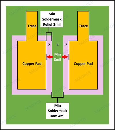
Solder Mask Clearance: The solder mask clearance is the distance between the edge of a copper pad and the edge of the solder mask opening. This clearance is necessary to account for any misalignment during the solder mask application process and to ensure that the entire pad is exposed for soldering. The clearance value depends on the PCB Manufacturer’s capabilities and the specific design requirements.
-
Solder Mask Sliver: A solder mask sliver is a thin strip of solder mask between two adjacent copper features, such as pads or traces. If the sliver is too narrow, it may break off during the manufacturing process or in the field, leading to short circuits or other issues. To avoid this, designers must adhere to the minimum solder mask sliver width specified by the PCB manufacturer.
-
Solder Mask Expansion: During the curing process, the solder mask may expand slightly. This expansion can cause the solder mask to encroach on the exposed copper areas, reducing the available space for soldering. To compensate for this, designers should follow the PCB manufacturer’s guidelines for minimum solder mask expansion allowances.
-
Solder Mask Color: While green is the most common solder mask color, other colors may be used for specific applications or to improve the PCB’s appearance. However, designers should be aware that different colors may have varying properties, such as UV light sensitivity or thermal expansion coefficients, which can affect the solder mask application process and the final PCB performance.
-
Solder Mask Thickness: The thickness of the solder mask can impact its electrical insulation properties, as well as its ability to protect the copper traces from damage. Designers should specify the desired solder mask thickness based on the PCB’s intended application and the manufacturer’s recommendations.
-
Solder Mask Surface Finish: The solder mask surface can be either glossy or matte, depending on the desired appearance and the specific manufacturing process used. A matte finish is often preferred for improved readability of text and markings on the PCB surface.

Advantages of Using Solder Mask
Using a solder mask in PCB manufacturing offers several benefits, including:
-
Improved Reliability: By preventing solder bridges and protecting the copper traces from damage, solder mask enhances the overall reliability of the PCB.
-
Better Electrical Insulation: The solder mask provides an additional layer of electrical insulation between copper traces and components, reducing the risk of short circuits and leakage currents.
-
Enhanced Durability: Solder mask protects the PCB from environmental factors such as moisture, dust, and chemicals, which can degrade its performance over time.
-
Increased Current Carrying Capacity: By insulating the copper traces, solder mask allows for closer trace spacing and wider traces, which can increase the current carrying capacity of the PCB.
-
Improved Appearance: Solder mask gives the PCB a clean, professional appearance and can be used to create text, logos, or other markings on the board’s surface.
-
Reduced Assembly Errors: The solder mask clearly defines the areas where components should be soldered, reducing the risk of assembly errors and improving the overall quality of the finished product.

Challenges and Limitations
While solder mask is an essential part of modern PCB manufacturing, there are some challenges and limitations to consider:
-
Minimum Feature Size: The resolution of the solder mask application process limits the minimum size of features that can be reliably created. This can be a challenge for designs with very fine pitch components or high-density layouts.
-
Alignment Accuracy: Misalignment between the solder mask and the copper features can lead to issues such as exposed copper or solder mask encroachment on pads. Proper process control and design for manufacturing (DFM) practices are necessary to minimize these issues.
-
Material Compatibility: Some solder mask materials may not be compatible with certain PCB substrates, Surface Finishes, or assembly processes. Designers must carefully select the solder mask material based on the specific requirements of the project.
-
Cost: Applying solder mask adds an additional step to the PCB manufacturing process, which can increase the overall cost of the board. However, the benefits of using solder mask often outweigh the added cost.
-
Repair and Rework: Solder mask can make it more difficult to repair or rework a PCB, as the mask must be removed to access the underlying copper features. This can be a time-consuming and delicate process.
Frequently Asked Questions (FAQ)
-
What is the purpose of solder mask on a PCB?
Answer: The primary purposes of solder mask are to prevent solder bridges from forming between closely spaced solder pads, protect the copper traces from oxidation and contamination, provide electrical insulation, improve the PCB’s appearance, and enhance the overall durability of the board. -
What are the most common colors for solder mask?
Answer: The most common color for solder mask is green, but other colors such as red, blue, black, and white are also available. The choice of color depends on the specific application and the desired appearance of the PCB. -
What is the difference between liquid photoimageable solder mask (LPSM) and dry film solder mask (DFSM)?
Answer: LPSM is applied as a liquid and then exposed to UV light, while DFSM is a solid film that is laminated onto the PCB surface. LPSM offers better thickness control and higher resolution, while DFSM provides excellent mechanical strength and chemical resistance. -
How does solder mask affect the assembly process?
Answer: Solder mask clearly defines the areas where components should be soldered, reducing the risk of assembly errors and improving the overall quality of the finished product. It also prevents solder bridges and protects the copper traces from damage during the assembly process. -
Can solder mask be removed for repair or rework?
Answer: Yes, solder mask can be removed for repair or rework, but it is a time-consuming and delicate process. The mask must be carefully removed to access the underlying copper features without causing damage to the PCB.
In conclusion, solder mask is a critical component in modern PCB manufacturing, offering numerous benefits such as improved reliability, better electrical insulation, enhanced durability, and increased current carrying capacity. By understanding the types, application processes, design considerations, and challenges associated with solder mask, PCB Designers and manufacturers can create high-quality, reliable circuit boards that meet the demanding requirements of today’s electronic devices.
No responses yet