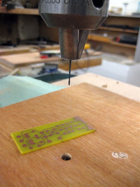
What are PCB Drilled Holes?
PCB drilled holes are openings created in a printed circuit board during the manufacturing process. These holes are typically made using specialized drilling machines that can create precise and uniform openings in the PCB substrate. The purpose of these holes is to allow the insertion of electronic components, enable electrical connections between layers, and facilitate the attachment of mechanical components.
Types of PCB Drilled Holes
There are several types of PCB drilled holes, each serving a specific purpose in the overall design and functionality of the circuit board. The main types of PCB drilled holes include:
- Through Holes
- Blind Vias
- Buried Vias
- Microvias
- Mechanical Holes
Let’s explore each type in more detail.
Through Holes
Through holes are the most common type of PCB drilled holes. As the name suggests, these holes pass completely through the PCB, from one side to the other. They are used primarily for mounting through-hole components, such as resistors, capacitors, and connectors. Through holes also enable electrical connections between layers of the PCB by allowing the component leads to pass through the board and be soldered on both sides.
Characteristics of Through Holes
- Pass completely through the PCB
- Used for mounting through-hole components
- Enable electrical connections between layers
- Typically larger in diameter compared to other types of holes
- Require more board space than surface-mount components
Applications of Through Holes
- Mounting through-hole components
- Providing electrical connections between layers
- Allowing the attachment of mechanical components, such as standoffs and connectors
Blind Vias
Blind vias are a type of PCB drilled hole that starts from one side of the board but does not pass through to the other side. Instead, they terminate at a specific inner layer of the PCB. Blind vias are used to establish electrical connections between the outer layer and one or more inner layers of the board.
Characteristics of Blind Vias
- Start from one side of the PCB and terminate at an inner layer
- Used for establishing electrical connections between outer and inner layers
- Require more precise drilling and plating processes compared to through holes
- Help reduce board size and improve signal integrity
Applications of Blind Vias
- Connecting surface-mount components to inner layers
- Reducing the size of the PCB by eliminating the need for through holes
- Improving signal integrity by minimizing the length of electrical connections
Buried Vias
Buried vias are PCB drilled holes that connect two or more inner layers of the board without extending to either of the outer layers. These vias are “buried” within the PCB stack-up and are not visible from the surface of the board. Buried vias are used to establish electrical connections between inner layers, allowing for more complex routing and higher circuit density.
Characteristics of Buried Vias
- Connect inner layers of the PCB without extending to the outer layers
- Used for establishing electrical connections between inner layers
- Require precise alignment and drilling processes
- Help increase circuit density and reduce board size
Applications of Buried Vias
- Connecting inner layers of the PCB for complex routing
- Increasing circuit density by utilizing the inner layers of the board
- Reducing signal interference by keeping high-speed signals on inner layers
Microvias
Microvias are small, high-precision PCB drilled holes with diameters typically less than 0.15mm (6 mils). These holes are laser-drilled and are used to establish electrical connections between adjacent layers in high-density PCB designs. Microvias are essential for advanced packaging technologies, such as High-Density Interconnect (HDI) PCBs.
Characteristics of Microvias
- Small diameter, typically less than 0.15mm (6 mils)
- Created using laser drilling techniques
- Used for establishing electrical connections between adjacent layers
- Enable high-density PCB designs and advanced packaging technologies
Applications of Microvias
- High-density PCB designs, such as HDI boards
- Connecting fine-pitch surface-mount components
- Enabling the use of advanced packaging technologies, such as chip-scale packages (CSPs) and ball grid arrays (BGAs)
Mechanical Holes
Mechanical holes are PCB drilled holes that serve a non-electrical purpose. These holes are used for attaching mechanical components, such as standoffs, mounting brackets, and heat sinks, to the PCB. Mechanical holes do not have any copper plating and are not used for electrical connections.
Characteristics of Mechanical Holes
- Used for attaching mechanical components to the PCB
- Do not have copper plating
- Not used for electrical connections
- Typically larger in diameter compared to other types of holes
Applications of Mechanical Holes
- Attaching standoffs and spacers for board support
- Mounting the PCB to an enclosure or chassis
- Attaching heat sinks for thermal management

PCB Drilled Hole Sizes and Tolerances
When designing and manufacturing PCBs, it is essential to consider the sizes and tolerances of the drilled holes. The hole size and tolerance will depend on the specific requirements of the components being used and the manufacturing capabilities of the PCB fabricator.
| Hole Type | Typical Diameter Range | Tolerance |
|---|---|---|
| Through Holes | 0.5mm – 1.0mm | ±0.1mm |
| Blind Vias | 0.2mm – 0.5mm | ±0.05mm |
| Buried Vias | 0.2mm – 0.5mm | ±0.05mm |
| Microvias | 0.1mm – 0.15mm | ±0.025mm |
| Mechanical Holes | 2.0mm – 5.0mm | ±0.2mm |
It is important to consult with your PCB manufacturer to ensure that your design meets their specific capabilities and requirements.

Frequently Asked Questions (FAQ)
-
What is the difference between through holes and vias?
Through holes pass completely through the PCB and are used for mounting components and providing electrical connections between layers. Vias, on the other hand, are used specifically for establishing electrical connections between layers and do not necessarily pass through the entire board. -
Can blind vias and buried vias be used in the same PCB?
Yes, blind vias and buried vias can be used together in the same PCB design. This combination allows for more complex routing and higher circuit density, as it enables the use of multiple inner layers for electrical connections. -
What are the advantages of using microvias in PCB design?
Microvias offer several advantages in PCB design, including: - Enabling high-density PCB layouts by allowing for finer pitch connections
- Reducing signal interference by keeping high-speed signals on inner layers
-
Facilitating the use of advanced packaging technologies, such as chip-scale packages (CSPs) and ball grid arrays (BGAs)
-
How do I choose the right hole size for my components?
When choosing the hole size for your components, consider the following factors: - The lead diameter of the component
- The required clearance between the lead and the hole wall
-
The manufacturing capabilities of your PCB fabricator
It is essential to consult with your PCB manufacturer and refer to the component datasheet to ensure that you select the appropriate hole size. -
Can mechanical holes be plated?
Mechanical holes are typically not plated, as they serve a non-electrical purpose. However, in some cases, mechanical holes may be plated to provide additional structural support or to improve the grounding of the PCB. If you require plated mechanical holes, discuss this requirement with your PCB manufacturer.

Conclusion
PCB drilled holes are a critical aspect of printed circuit board design and manufacturing. The various types of holes, including through holes, blind vias, buried vias, microvias, and mechanical holes, serve different purposes and enable the creation of complex, high-density PCBs. Understanding the characteristics and applications of each type of hole is essential for designing and manufacturing reliable and efficient electronic devices.
When designing your PCB, consider the specific requirements of your components, the desired circuit density, and the manufacturing capabilities of your PCB fabricator. By carefully selecting the appropriate types of drilled holes and their sizes, you can ensure that your PCB meets the performance and reliability standards required for your application.
No responses yet