What is PCB Gold-Plating?
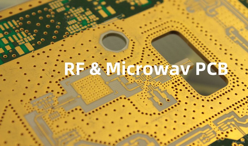
PCB gold-plating is the process of selectively depositing a thin layer of gold onto specific areas of a printed circuit board (PCB). Gold plating is commonly used on PCBs to enhance the connectivity, durability, and performance of the board’s surface and components. The gold layer provides excellent electrical conductivity, corrosion resistance, and improved solderability for the PCB.
Benefits of Gold Plating PCBs
- Enhanced electrical conductivity
- Superior corrosion resistance
- Improved solderability and wettability
- Increased durability and wear resistance
- Better heat dissipation and thermal management
- Compatibility with wire bonding and other assembly processes
Selective Gold Plating Techniques
There are several methods for selectively applying gold plating to PCBs. The choice of technique depends on factors such as the desired plating thickness, the size and geometry of the plated features, and the production volume. Here are some common selective gold plating techniques:
Electroplating
Electroplating is a widely used method for selectively depositing gold onto PCBs. In this process, the PCB is immersed in a gold electrolyte solution, and an electric current is applied to plate the exposed metal surfaces. A photoresist mask is used to define the areas to be plated, while the rest of the board is protected. Electroplating allows for precise control over the plating thickness and can achieve high-quality, uniform gold layers.
Immersion Gold Plating
Immersion gold plating, also known as electroless gold plating, is a chemical process that deposits a thin layer of gold onto exposed copper surfaces without the need for an external electric current. The PCB is immersed in a gold solution containing a reducing agent, which triggers a chemical reaction that causes the gold to adhere to the copper. Immersion gold plating is commonly used as a surface finish for PCBs, providing good solderability and corrosion resistance.
Brush Plating
Brush plating, or selective brush plating, is a manual technique that involves applying gold plating solution to specific areas of the PCB using a brush or swab. This method is suitable for small-scale production or repair work, as it allows for targeted gold plating without the need for masking or immersion. However, brush plating requires skilled operators and may result in less uniform plating compared to other techniques.
Spot Plating
Spot plating is a selective gold plating technique that uses a localized plating tool to deposit gold onto specific areas of the PCB. The plating tool, which can be a pen-like device or a small nozzle, directs the gold electrolyte solution onto the desired locations while an electric current is applied. Spot plating offers high precision and can be automated for faster production, making it suitable for medium to high-volume applications.
Factors Affecting Gold Plating Quality
To ensure high-quality gold plating on PCBs, several factors must be considered:
Surface Preparation
Proper surface preparation is crucial for achieving good adhesion and uniformity of the gold plating. The PCB surface should be cleaned thoroughly to remove any contaminants, oxides, or residues that may interfere with the plating process. This can be done through chemical cleaning, micro-etching, or plasma treatment, depending on the specific requirements of the board.
Plating Thickness
The thickness of the gold plating layer affects the performance and durability of the PCB. Thicker gold layers provide better wear resistance and corrosion protection but may increase the cost and processing time. The choice of plating thickness depends on the specific application and the desired balance between performance and cost.
| Application | Recommended Gold Plating Thickness |
|---|---|
| General purpose | 0.05 – 0.10 μm |
| High-reliability | 0.25 – 0.50 μm |
| Wire bonding | 0.75 – 1.50 μm |
| Extreme environments | 1.50 – 2.50 μm |
Plating Solution Composition
The composition of the gold plating solution plays a significant role in the quality and properties of the deposited gold layer. The solution should contain the appropriate concentration of gold ions, as well as additives that promote uniform deposition, improve adhesion, and control the plating rate. Regular monitoring and maintenance of the plating solution are essential to ensure consistent results.
Current Density
In electroplating processes, the current density determines the rate of gold deposition and affects the uniformity and morphology of the plated layer. Higher current densities generally result in faster plating rates but may lead to non-uniform deposition or surface defects. It is important to optimize the current density based on the specific plating solution, PCB geometry, and desired plating characteristics.
Temperature Control
Temperature control is critical for maintaining the stability and performance of the gold plating process. The plating solution should be maintained at the optimal temperature range specified by the solution manufacturer. Higher temperatures can increase the plating rate but may also cause excessive evaporation or degradation of the solution. Proper temperature control ensures consistent plating quality and minimizes process variability.

Design Considerations for Gold-Plated PCBs
When designing PCBs for selective gold plating, several factors should be taken into account to ensure optimal performance and manufacturability:
Pad and Trace Geometry
The size and shape of the pads and traces to be gold-plated should be designed to accommodate the plating process. Adequate spacing between features is necessary to prevent bridging or short circuits during plating. The aspect ratio of plated holes should also be considered to ensure uniform coverage and avoid plating voids.
Soldermask and Silkscreen
The soldermask and silkscreen layers should be designed to expose only the areas intended for gold plating. Accurate registration and alignment of these layers are crucial for achieving precise selective plating. The soldermask should also provide adequate protection for the non-plated areas of the PCB during the plating process.
Material Compatibility
The choice of PCB Substrate material and the compatibility of the gold plating process should be considered. Some substrate materials may require additional surface treatments or adhesion promoters to ensure good bonding of the gold layer. The thermal expansion properties of the substrate and the gold plating should also be matched to minimize stress and delamination during temperature cycling.
Electrical Performance
The impact of gold plating on the electrical performance of the PCB should be evaluated. While gold provides excellent electrical conductivity, its thickness and coverage can affect the impedance and Signal Integrity of high-frequency circuits. Careful design and simulation of the plated features are necessary to optimize the electrical performance of the PCB.
Quality Control and Testing
To ensure the quality and reliability of gold-plated PCBs, various inspection and testing methods are employed:
Visual Inspection
Visual inspection is the first line of quality control for gold-plated PCBs. The plated surfaces should be examined for uniformity, coverage, and the absence of defects such as voids, pinholes, or delamination. Microscopic inspection may be necessary to detect smaller defects or evaluate the plating thickness.
Adhesion Testing
Adhesion testing is performed to assess the bond strength between the gold plating and the underlying substrate. Common adhesion tests include the tape test, where a pressure-sensitive tape is applied and removed to check for plating delamination, and the scratch test, where a controlled force is used to create a scratch on the plated surface to evaluate adhesion.
Thickness Measurement
Measuring the thickness of the gold plating layer is important for ensuring compliance with the specified requirements. Various methods can be used, such as X-ray fluorescence (XRF) spectroscopy, beta backscatter, or cross-sectional analysis. These techniques provide accurate thickness measurements and help verify the uniformity of the plating across the PCB.
Solderability Testing
Solderability testing is conducted to evaluate the ability of the gold-plated surfaces to be wetted by solder and form reliable solder joints. The wetting balance test is a common method, where the plated surface is dipped into molten solder, and the wetting force and time are measured. Other methods include the dip-and-look test and the surface insulation resistance (SIR) test.
Environmental Testing
Environmental testing is performed to assess the durability and reliability of gold-plated PCBs under various environmental conditions. These tests may include thermal cycling, humidity exposure, salt spray corrosion, and mechanical shock and vibration. The plated surfaces are evaluated for any signs of degradation, such as cracking, delamination, or corrosion, to ensure they can withstand the intended operating conditions.
Frequently Asked Questions (FAQ)
1. What are the advantages of selective gold plating over full gold plating?
Selective gold plating offers several advantages over full gold plating:
– Cost savings: By plating only the specific areas that require gold, the overall cost of the PCB is reduced compared to full gold plating.
– Targeted performance: Selective plating allows for the optimization of gold thickness and coverage based on the specific requirements of each area, ensuring optimal performance where needed.
– Compatibility with other Surface Finishes: Selective gold plating can be combined with other surface finishes, such as ENIG or OSP, on the same PCB, providing flexibility in design and assembly.
2. How does gold plating thickness affect the performance of the PCB?
The thickness of the gold plating layer has a significant impact on the performance and durability of the PCB:
– Thicker gold layers provide better wear resistance and corrosion protection, making them suitable for high-reliability applications or harsh environments.
– Thinner gold layers are more cost-effective and sufficient for general-purpose applications with moderate performance requirements.
– The choice of plating thickness should be based on the specific application, considering factors such as the operating conditions, expected lifecycle, and cost constraints.
3. Can selective gold plating be applied to both through-hole and surface-mount components?
Yes, selective gold plating can be applied to both through-hole and surface-mount components on PCBs:
– For through-hole components, gold plating is commonly used on the contact fingers or connector pins to enhance electrical conductivity and corrosion resistance.
– For surface-mount components, gold plating is often applied to the pads or contacts to improve solderability and ensure reliable solder joint formation.
4. How does the choice of PCB substrate material affect the gold plating process?
The choice of PCB substrate material can have an impact on the gold plating process:
– Different substrate materials may require specific surface preparation methods or adhesion promoters to ensure good bonding of the gold layer.
– The thermal expansion properties of the substrate should be considered to minimize stress and delamination during temperature cycling.
– Some substrate materials, such as high-frequency laminates, may have specific requirements for gold plating to maintain their electrical performance.
5. What are the common defects encountered in gold-plated PCBs, and how can they be prevented?
Common defects in gold-plated PCBs include:
– Voids or pinholes: These can be caused by improper surface preparation, contamination, or inadequate plating parameters. Proper cleaning, optimized plating conditions, and quality control measures can help prevent these defects.
– Non-uniform plating: Uneven gold thickness or coverage can result from poor current distribution, incorrect plating solution composition, or inadequate agitation. Proper setup and monitoring of the plating process can ensure uniform plating.
– Delamination: Poor adhesion between the gold layer and the substrate can lead to delamination. Adequate surface preparation, compatible materials, and controlled plating parameters can minimize the risk of delamination.
– Brittle or cracked plating: Excessive internal stress or incorrect plating conditions can cause the gold layer to become brittle or crack. Optimizing the plating process and controlling the plating rate can help prevent these issues.
By understanding the causes of these defects and implementing appropriate process controls and quality assurance measures, manufacturers can minimize their occurrence and ensure the production of high-quality gold-plated PCBs.

No responses yet