Introduction to PCB through-holes
Printed circuit boards (PCBs) are the backbone of modern electronics. They provide a way to mechanically support and electrically connect electronic components using conductive pathways, tracks, or signal traces etched from copper sheets laminated onto a non-conductive substrate. One key feature of PCBs is the use of through-holes to create electrical connections between different layers of the board.
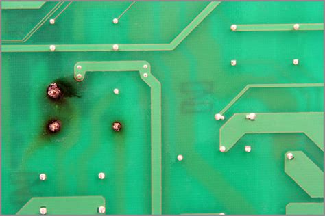
PCB through-holes, also known as plated through-holes (PTHs), are small holes drilled through a printed circuit board that are then coated or plated with a conductive material, typically copper, to create an electrical connection between the different layers of the PCB. These holes allow components to be mounted on both sides of the board and enable more complex circuitry to be designed in a smaller footprint.
Types of PCB Through-Holes
There are several types of through-holes used in PCB design, each serving a specific purpose:
1. Component Through-Holes
Component through-holes are used to mount through-hole components, such as resistors, capacitors, and inductors, to the PCB. These holes are typically larger than other types of through-holes to accommodate the component leads. The leads are inserted through the holes and then soldered to the copper pads on the opposite side of the board to create a secure mechanical and electrical connection.
2. Via Through-Holes
Via through-holes, or simply vias, are used to create electrical connections between different layers of a multi-layer PCB. They allow signals to pass from one layer to another, enabling more complex routing and circuitry in a smaller area. Vias come in several types:
- Through vias: These vias pass through all layers of the PCB, from the top to the bottom.
- Blind vias: These vias start at an outer layer and terminate at an inner layer, without passing through the entire board.
- Buried vias: These vias connect inner layers without reaching either the top or bottom layer of the PCB.
3. Mounting Through-Holes
Mounting through-holes are used to secure the PCB to an enclosure or chassis using screws, standoffs, or other hardware. These holes are typically larger than component or via through-holes and do not have any electrical function.

PCB Through-Hole Manufacturing Process
The process of creating through-holes in a PCB involves several steps:
-
Drilling: Small holes are drilled through the PCB substrate at the desired locations using a computer-controlled drill machine. The drill bit size and type are selected based on the required hole diameter and the material of the substrate.
-
Deburring: After drilling, the holes are deburred to remove any rough edges or debris that could interfere with the plating process or cause electrical issues.
-
Cleaning: The drilled and deburred board is then cleaned to remove any contaminants or residues that could affect the plating process.
-
Electroless copper deposition: The board is immersed in a chemical bath that deposits a thin layer of copper onto the walls of the drilled holes and the surface of the board. This process is called electroless copper deposition and creates a conductive base layer for the subsequent electrolytic plating step.
-
Electrolytic copper plating: The board is then placed in an electrolytic plating bath, where an electric current is applied to deposit a thicker layer of copper onto the walls of the holes and the surface of the board. This process ensures a strong, reliable electrical connection between the layers of the PCB.
-
Finishing: After plating, the board may undergo additional finishing processes, such as solder mask application, silkscreen printing, and surface finish application (e.g., HASL, ENIG, or immersion silver), depending on the specific requirements of the design.

Advantages of Using Through-Holes in PCB Design
Using through-holes in PCB design offers several advantages:
-
Mechanical stability: Through-hole components provide a stronger mechanical connection to the PCB compared to surface-mount components, making them ideal for applications that require high reliability or are subject to vibration or mechanical stress.
-
Simplified assembly: Through-hole components are easier to assemble manually compared to surface-mount components, as they can be inserted through the holes and soldered in place using simple tools and techniques.
-
Improved thermal management: Through-hole components can dissipate heat more effectively than surface-mount components, as the leads of the component extend through the board and can be connected to thermal planes or heatsinks on the opposite side.
-
Enhanced current-carrying capacity: Through-hole vias can carry higher currents compared to surface traces, as the plated hole provides a larger cross-sectional area for current flow.
-
Compatibility with legacy components: Many older electronic components and connectors are only available in through-hole packages, making through-holes essential for designs that need to incorporate these legacy components.

Disadvantages of Using Through-Holes in PCB Design
Despite their advantages, using through-holes in PCB design also has some drawbacks:
-
Increased board size: Through-hole components require more space on the PCB compared to surface-mount components, as the holes and pads take up additional room. This can lead to larger board sizes and reduced component density.
-
Higher manufacturing costs: Drilling and plating through-holes add additional steps to the PCB manufacturing process, which can increase production time and costs compared to designs that use only surface-mount components.
-
Limited routing options: Through-holes can obstruct the routing of traces on inner layers of the PCB, as the holes must be avoided when designing the circuit layout. This can lead to more complex and less efficient routing, especially in dense designs.
-
Reduced high-frequency performance: Through-holes can create unwanted stubs or resonances that can degrade high-frequency signal performance, particularly in designs operating at microwave or millimeter-wave frequencies.
Guidelines for Designing with PCB Through-Holes
When incorporating through-holes in your PCB design, consider the following guidelines:
-
Hole size: Ensure that the hole size is appropriate for the component leads or via requirements. Holes that are too small can make it difficult to insert components or achieve reliable plating, while holes that are too large can waste board space and reduce mechanical stability.
-
Pad size: Provide sufficient pad size around the holes to ensure good solderability and mechanical strength. The pad should be large enough to accommodate any misalignment during component placement and provide enough surface area for a strong solder joint.
-
Hole placement: Position holes and vias strategically to minimize their impact on signal routing and to avoid interference with other components or features on the board. Follow the manufacturer’s recommendations for minimum hole spacing and distance from board edges.
-
Plating thickness: Specify an appropriate plating thickness for the holes based on the electrical and mechanical requirements of the design. Thicker plating can improve current-carrying capacity and mechanical stability but may increase manufacturing costs.
-
Via types: Select the appropriate via type (through, blind, or buried) based on the complexity of the design and the number of layers in the PCB. Blind and buried vias can enable more dense routing but may increase manufacturing costs and complexity.
-
Thermal management: Consider the thermal requirements of through-hole components and design the PCB layout accordingly. Provide sufficient copper area around the holes for heat dissipation and consider the use of thermal vias or planes to transfer heat away from sensitive components.
PCB Through-Hole Design Considerations
When designing a PCB with through-holes, several factors should be taken into account to ensure optimal performance, reliability, and manufacturability:
1. Aspect Ratio
The aspect ratio of a through-hole refers to the ratio of the hole depth to its diameter. In general, a higher aspect ratio makes it more challenging to achieve reliable plating and increases the risk of voids or other defects in the hole. The maximum aspect ratio that can be reliably manufactured depends on the capabilities of the PCB fabricator and the specific plating process used.
As a general guideline, aim for an aspect ratio of 8:1 or less for standard through-holes, and 10:1 or less for high-reliability applications. If your design requires higher aspect ratios, consult with your PCB manufacturer to determine the feasibility and any additional costs or lead times associated with the more challenging manufacturing process.
2. Annular Ring
The annular ring is the copper pad that surrounds a through-hole on the PCB surface. A sufficient annular ring is essential for ensuring good solderability and mechanical stability of the component or via. The minimum annular ring size depends on the hole diameter and the manufacturing tolerances of the PCB fabricator.
As a rule of thumb, aim for an annular ring width of at least 0.25 mm (10 mils) for standard through-holes, and 0.5 mm (20 mils) for high-reliability applications. Larger annular rings can provide additional mechanical strength and facilitate manual soldering, but they may also increase the overall board size and reduce the available routing space.
3. Drill Breakout
Drill breakout refers to the phenomenon where the drilling process causes the copper pad around a hole to be partially or completely removed, resulting in a weakened or broken connection. This can occur due to misalignment between the drill bit and the pad, or due to excessive vibration or wear of the drilling equipment.
To minimize the risk of drill breakout, ensure that the annular ring is sufficiently large and that the drill hit location is centered on the pad. Avoid placing holes too close to the edge of the board or other features that could interfere with the drilling process. If drill breakout is a concern, consider using larger pads or specifying a higher-quality drilling process with tighter tolerances.
4. Via Tenting
Via tenting refers to the practice of covering the top and/or bottom of a via with solder mask to prevent solder from flowing into the hole during the assembly process. Tenting can help to prevent solder bridging between adjacent vias or components and can also provide additional insulation and protection for the via.
When designing vias for tenting, ensure that the solder mask aperture is slightly larger than the via hole to allow for proper coverage. The minimum solder mask expansion depends on the capabilities of the PCB fabricator but is typically in the range of 0.1 to 0.15 mm (4 to 6 mils).
Keep in mind that tenting can make it more difficult to inspect or repair the via connection, as the solder joint is hidden under the solder mask. In some cases, it may be preferable to leave the via untented or to use a clear solder mask to allow for visual inspection.
5. Electrical Clearance
Electrical clearance refers to the minimum distance between conductive features on the PCB, such as traces, pads, and vias, to prevent electrical shorts or arcing. The required clearance depends on the voltage and current levels of the signals, as well as the manufacturing tolerances and the dielectric strength of the PCB material.
For through-holes, ensure that there is sufficient clearance between the hole and any adjacent conductive features, both on the surface of the board and on inner layers. The minimum clearance should be based on the maximum voltage differential between the features and should account for any potential misalignment or deformation of the hole during the manufacturing process.
As a general guideline, aim for a minimum clearance of 0.25 mm (10 mils) between through-holes and other conductive features for standard low-voltage applications, and 0.5 mm (20 mils) or more for high-voltage or high-reliability applications. Consult with your PCB manufacturer and refer to industry standards, such as IPC-2221, for specific clearance requirements based on your design parameters.
PCB Through-Hole Testing and Inspection
To ensure the quality and reliability of through-holes in a PCB, several testing and inspection methods can be employed during the manufacturing process:
1. Visual Inspection
Visual inspection is the most basic and straightforward method of checking the quality of through-holes. This involves examining the holes under magnification to look for any visible defects, such as voids, cracks, or incomplete plating. Visual inspection can be performed manually by a trained operator or automatically using machine vision systems.
2. Automated Optical Inspection (AOI)
AOI uses high-resolution cameras and image processing software to automatically inspect the PCB for a variety of defects, including issues with through-holes. AOI systems can quickly scan the entire board and compare the images to a predefined set of criteria, flagging any holes that fall outside the acceptable range. This method is faster and more consistent than manual visual inspection but may not be able to detect all types of defects.
3. X-Ray Inspection
X-ray inspection uses high-energy radiation to create a detailed image of the internal structure of the PCB, including the through-holes. This method can detect defects that may not be visible on the surface, such as voids or inclusions in the plating, or misalignment of the holes between layers. X-ray inspection is particularly useful for evaluating the quality of blind or buried vias, which cannot be easily inspected using other methods.
4. Microsectioning
Microsectioning involves physically cutting the PCB along a through-hole and examining the cross-section under a microscope. This destructive testing method provides a detailed view of the plating quality and thickness, as well as any defects or anomalies in the hole structure. Microsectioning is typically used for process validation or failure analysis, rather than for routine quality control.
5. Electrical Testing
Electrical testing involves measuring the resistance, continuity, and insulation resistance of the through-holes to ensure that they meet the specified electrical requirements. This can be done using automated test equipment (ATE) or manual probing methods. Electrical testing can detect issues such as open or short circuits, high-resistance connections, or leakage between adjacent holes.
By employing a combination of these testing and inspection methods, PCB manufacturers can ensure that the through-holes in their products meet the required quality standards and are free from defects that could compromise the reliability or performance of the final assembly.
Frequently Asked Questions (FAQ)
-
What is the difference between a through-hole and a via?
A through-hole is a general term for any hole that is drilled through a PCB and plated with a conductive material. Vias are a specific type of through-hole that are used to create electrical connections between different layers of the PCB, allowing signals to pass from one layer to another. -
Can through-holes be used for components and vias in the same design?
Yes, a PCB design can incorporate both component through-holes and vias as needed. Component through-holes are typically larger and are used to mount through-hole components, while vias are smaller and are used for inter-layer connections. -
What is the minimum hole size that can be reliably manufactured?
The minimum hole size depends on the capabilities of the PCB fabricator and the specific manufacturing process used. As a general guideline, most PCB manufacturers can reliably produce through-holes down to 0.2 mm (8 mils) in diameter, while some advanced processes can achieve hole sizes as small as 0.1 mm (4 mils). -
How does the plating thickness affect the performance of a through-hole?
The plating thickness of a through-hole determines its electrical and mechanical properties. Thicker plating can improve the current-carrying capacity and mechanical strength of the hole but may also increase the manufacturing cost and the risk of defects. The optimal plating thickness depends on the specific requirements of the design and should be specified based on industry standards and guidance from the PCB manufacturer. -
Can through-holes be used in High-Frequency PCB designs?
Through-holes can be used in high-frequency PCB designs but may require special considerations to minimize their impact on signal integrity. At high frequencies, through-holes can create unwanted stubs or resonances that can distort or attenuate the signals. To mitigate these effects, designers may need to use smaller hole sizes, shorter stub lengths, or specialized via structures, such as blind or buried vias, that minimize the discontinuities in the signal path. Careful simulation and testing should be conducted to ensure that the through-holes do not degrade the high-frequency performance of the design.
By understanding the key aspects of PCB through-holes, including their types, manufacturing process, design considerations, and testing methods, engineers and designers can create more reliable, efficient, and cost-effective PCBs that meet the demands of today’s complex electronic systems.
No responses yet