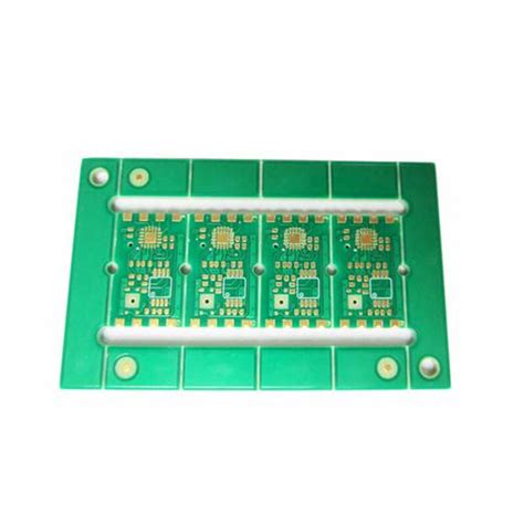
What are Castellations on a PCB?
Castellations, also known as castellated holes or castellated edges, are a type of edge connector used on printed circuit boards (PCBs). They consist of a series of semi-circular cut-outs or plated half-holes along the edge of a PCB. These castellations allow the board to be easily connected to other PCBs or components by soldering, effectively acting as both a mechanical and electrical connection point.
Castellated PCBs offer several advantages over traditional connectors:
– Lower profile and smaller footprint
– Easier assembly and rework
– Increased reliability and durability
– Lower cost at volume
How are Castellated Holes Made?
The castellations are typically made during the PCB fabrication process:
-
The PCB panel is drilled or routed with a series of evenly spaced holes along the edge where the castellations will be located. The holes are centered on the edge of the board.
-
Copper plating is applied through the holes to create electrical connections. This plating also covers the walls of the drilled holes.
-
The panel is then cut or routed down the center of each hole. This exposes the plated half-holes, creating the distinct semi-circular castellated edge.
-
Finally, a surface finish like ENIG or HASL is applied to protect the exposed copper and enhance solderability.
The size and spacing of the castellations depends on the requirements of the design. Common configurations include:
| Pitch (mm) | Drill Size (mm) | Castellation Width (mm) |
|---|---|---|
| 1.0 | 0.7 | 0.8 |
| 1.27 | 1.0 | 1.0 |
| 2.0 | 1.5 | 1.6 |
| 2.54 | 2.0 | 2.2 |
Table 1. Common Castellation Configurations

Design Considerations for Castellated PCBs
Mechanical Strength
Since the castellations remove material from the edge of the board, it’s important to consider the impact on mechanical strength. For boards that may experience significant stresses, using more or larger castellations can help maintain rigidity. Supporting the castellated edge with a stiffener or enclosure can also prevent flexing and damage.
Electrical Requirements
The electrical characteristics of the castellated connections must be suitable for the signals being transmitted. High-speed signals may require impedance control, while power delivery requires sufficient current carrying capacity.
The plating and surface finish on the castellations should be selected based on the connection type and operating environment. For example, ENIG provides a durable surface for repeated mating cycles, while HASL offers good solderability for permanent connections.
Assembly and Rework
Castellated PCBs are often easier to assemble than those with traditional connectors, since the connections can be made with standard SMT processes. However, special fixturing may be required to hold the board in alignment during reflow.
If rework is required, castellated connections can typically be desoldered and repaired more easily than press-fit or adhesive-bonded connectors. The open configuration allows better access for tools and inspection.

Applications for Castellated PCBs
Board-to-Board Connections
One of the most common uses for castellated PCBs is in board-to-board connections. The castellations allow two PCBs to be soldered together at a 90-degree angle, creating a compact and robust connection without additional connectors.
This is often used in module-on-board designs, where a smaller daughterboard is mounted perpendicularly on a motherboard. The castellations provide both the mechanical attachment and electrical interconnect between the boards. Examples include:
- RF modules
- Sensor boards
- Mezzanine cards
- Plug-in modules
Edge Connectors
Castellations can also act as edge connectors, allowing the PCB to plug into a socket or backplane. In this case, the castellations mate with spring contacts in the socket, rather than being soldered.
This allows the PCB to be easily installed and removed without tools or soldering. It provides a lower-profile and more compact alternative to traditional card-edge connectors.
Edge castellations are commonly found in:
- Blade servers
- Rack-mount systems
- Industrial controls
- Automotive electronics
Component Mounting
Some specialized components, like antenna modules or sensors, may have castellated edges that allow them to be directly soldered to a carrier PCB. This eliminates the need for an additional connector or housing.
The component’s castellations are typically spaced to match the land pattern on the PCB. The two are then aligned and soldered using a standard reflow process. This provides a simple and low-cost assembly method for these types of devices.

Advantages of Castellated PCBs
Space Savings
One of the key benefits of using castellations is the space savings compared to traditional connectors. The castellations have a much smaller footprint, allowing for denser PCB layouts. In applications where size is critical, such as mobile devices or wearables, castellated PCBs can provide significant advantages.
Cost Reduction
Castellated PCBs can also offer cost savings, particularly at higher volumes. The castellations are formed as an integral part of the PCB fabrication process, eliminating the need for separate connector components. This reduces both the bill of materials cost and the assembly cost.
In addition, castellated connections are typically more reliable than mechanical connectors, which can reduce warranty and repair costs over the product lifecycle. However, for very low volume projects, the additional setup and tooling costs for castellated PCBs may outweigh the savings.
Design Flexibility
Castellations provide designers with more flexibility in terms of PCB shape and layout. Since the castellation spacing is determined by the PCB design, it can be optimized for the specific requirements of the project. Unusual board shapes or cut-outs can be accommodated more easily than with fixed-pitch connectors.
Castellated edges also allow for more modular and reconfigurable designs. Boards can be swapped or upgraded without changing the base system. This can be particularly valuable in development and prototyping, where designs may go through multiple iterations.
Challenges and Limitations
Alignment and Soldering
One potential challenge with castellated PCBs is ensuring proper alignment during assembly. Since the castellations are typically quite small, even a slight misalignment can cause open or shorted connections.
Specialized fixturing is often used to hold the PCB in place during soldering. Visual alignment marks on the PCB can also aid in proper placement. In some cases, a stencil may be used to apply solder paste to the castellations prior to reflow.
Careful control of the soldering process is also critical. Too little solder can result in weak or open connections, while too much can cause bridging between adjacent castellations. Using a controlled-volume dispensing system or solder preforms can help ensure consistent results.
Signal Integrity
For high-speed or high-frequency signals, the castellated connections can present some signal integrity challenges. The discontinuity created by the castellated edge can cause reflections and impedance mismatches.
Careful design of the PCB layout and stack-up can help minimize these issues. Techniques like impedance matching, ground stitching, and length matching can be used to optimize the castellated connections for high-speed signals.
In some cases, additional components like choke coils or termination resistors may need to be placed close to the castellations to maintain signal integrity. Simulation and testing are often used to validate the performance of these critical interfaces.
Frequently Asked Questions
Q: Can castellated holes be used with through-hole components?
A: Castellations are primarily used for surface-mount connections, as the component leads need to be soldered to the plated semi-circles. Through-hole components typically require a full drilled hole. However, in some cases, the leads of through-hole parts can be bent to align with castellations for soldering.
Q: Are castellated PCBs more expensive than those with connectors?
A: It depends on the specific design and volume. For simple designs in high volumes, castellated PCBs can offer significant cost savings by eliminating separate connector components. However, for complex, low-volume designs, the additional setup and processing costs for castellations may be higher than using off-the-shelf connectors.
Q: Can castellated PCBs be disassembled for repair?
A: Yes, one of the advantages of castellated connections is that they can be desoldered for rework or repair. With proper techniques, the castellated board can be removed, repaired, and resoldered. However, repeated rework cycles can degrade the castellation plating and reduce reliability.
Q: What is the minimum pitch for castellated holes?
A: The minimum castellation pitch is typically around 0.8mm, which allows for a 0.5mm drill and 0.65mm pad. Tighter pitches are possible with advanced PCB fabrication techniques, but may increase cost and decrease reliability. The specific minimum pitch will depend on the capabilities of the PCB manufacturer.
Q: Are there any standards for castellated PCB design?
A: There are no universal standards for castellated PCBs, as the design is often application-specific. However, some industries or form factors may have de facto standards for castellation pitch and dimensions. For example, many blade server designs use a common pitch for interchangeaBLE Modules. Following industry best practices for PCB layout and manufacturability is always recommended.
Conclusion
Castellated PCBs offer a versatile and cost-effective solution for a wide range of interconnect challenges. By leveraging the inherent capabilities of the PCB fabrication process, castellations can provide high-density, high-reliability connections in a compact form factor.
However, castellated designs do require careful consideration of the mechanical, electrical, and manufacturing implications. Designers must balance the trade-offs between cost, performance, and reliability for each specific application.
As PCB technology continues to advance, castellated interconnects are becoming an increasingly attractive option for space-constrained and high-density designs. With proper planning and execution, castellated PCBs can provide a robust and efficient solution for many of today’s complex electronIC Packaging challenges.
No responses yet