Introduction to the IRF3205
The IRF3205 is a high-performance N-Channel MOSFET designed for efficient power switching and amplification. It offers a combination of low on-resistance, fast switching speeds, and high current handling capabilities, making it suitable for a wide range of power electronic applications.
Key Features of the IRF3205
-
Low on-resistance (RDS(on)): The IRF3205 exhibits a low on-resistance, typically around 8 mΩ, which minimizes conduction losses and improves efficiency in power switching applications.
-
High current handling: With a continuous drain current rating of 110 A, the IRF3205 is capable of handling high currents, making it suitable for demanding power applications.
-
Fast switching speeds: The IRF3205 offers fast switching characteristics, with low rise and fall times, enabling high-frequency operation and reducing switching losses.
-
Rugged design: The device features a rugged design with a high avalanche energy rating, providing enhanced reliability and robustness in demanding environments.
IRF3205 Datasheet Overview
The IRF3205 datasheet provides detailed information about the device’s electrical characteristics, package dimensions, and application guidelines. Let’s explore the key sections of the datasheet.
Absolute Maximum Ratings
The absolute maximum ratings section specifies the limits beyond which the device may experience permanent damage or degraded performance. Some essential parameters include:
| Parameter | Symbol | Value | Unit |
|---|---|---|---|
| Drain-Source Voltage | VDS | 55 | V |
| Gate-Source Voltage | VGS | ±20 | V |
| Continuous Drain Current (T_C=25°C) | ID | 110 | A |
| Pulsed Drain Current | IDM | 440 | A |
| Maximum Power Dissipation | PD | 200 | W |
| Operating Junction Temperature | T_J | -55 to 175 | °C |
| Storage Temperature | T_STG | -55 to 175 | °C |
It is crucial to adhere to these maximum ratings to ensure reliable operation and prevent device failure.
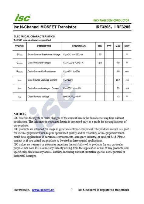
Electrical Characteristics
The electrical characteristics section provides detailed information about the device’s performance parameters under specific operating conditions. Some key parameters include:
| Parameter | Symbol | Conditions | Min | Typ | Max | Unit |
|---|---|---|---|---|---|---|
| Drain-Source Breakdown Voltage | BV_DSS | VGS=0V, ID=250µA | 55 | – | – | V |
| Gate Threshold Voltage | V_GS(th) | VDS=VGS, ID=250µA | 2.0 | – | 4.0 | V |
| Static Drain-Source On-Resistance (T_J=25°C) | RDS(on) | VGS=10V, ID=55A | – | 8.0 | 10.0 | mΩ |
| Input Capacitance | C_iss | VDS=25V, VGS=0V, f=1MHz | – | 3600 | – | pF |
| Output Capacitance | C_oss | VDS=25V, VGS=0V, f=1MHz | – | 360 | – | pF |
These parameters help designers understand the device’s performance under various operating conditions and aid in proper circuit design and component selection.
Package Information
The package information section provides the mechanical dimensions and pinout configuration of the IRF3205. The device is available in various package options, such as TO-220AB and D2PAK. The package dimensions are critical for ensuring proper PCB layout and heatsink selection.

Application Considerations
When designing circuits using the IRF3205, several application considerations should be taken into account to ensure optimal performance and reliability.
Gate Drive Requirements
The IRF3205 requires a suitable gate drive circuit to ensure efficient switching and minimize power losses. The gate drive should provide sufficient voltage and current to charge and discharge the device’s input capacitance quickly. A typical gate-source voltage of 10 V is recommended for optimal performance.
Heatsinking and Thermal Management
Due to the high power dissipation capability of the IRF3205, proper heatsinking is essential to maintain the device within its safe operating temperature range. The thermal resistance from junction to case (R_θJC) and junction to ambient (R_θJA) should be considered when selecting an appropriate heatsink. The datasheet provides information on the device’s thermal characteristics and maximum allowable junction temperature.
Paralleling Devices
In applications requiring higher current handling capabilities, multiple IRF3205 devices can be paralleled to share the load current. When paralleling devices, it is important to ensure proper current sharing by matching the on-resistance and thermal characteristics of the devices. The use of source ballast resistors can help balance the current distribution among the paralleled devices.
Protection Considerations
To enhance the reliability and protect the IRF3205 from potential damage, several protection measures can be implemented:
-
Gate-source protection: A zener diode or a voltage clamp circuit can be used to limit the gate-source voltage within the specified range, preventing gate oxide breakdown.
-
Drain-source overvoltage protection: Snubber Circuits or transient voltage suppressors can be employed to limit voltage spikes across the drain-source terminals during switching transitions.
-
Overcurrent protection: Current sensing techniques, such as using a shunt resistor or a current transformer, can be implemented to detect and limit excessive drain currents.

Frequently Asked Questions (FAQ)
-
What is the maximum drain-source voltage rating of the IRF3205?
The maximum drain-source voltage rating of the IRF3205 is 55 V. -
What is the typical on-resistance of the IRF3205?
The typical on-resistance (RDS(on)) of the IRF3205 is 8 mΩ when VGS=10V and ID=55A at a junction temperature of 25°C. -
Can the IRF3205 be used in parallel for higher current applications?
Yes, multiple IRF3205 devices can be paralleled to share the load current. Proper current sharing techniques, such as using source ballast resistors, should be employed to ensure equal current distribution among the devices. -
What is the maximum continuous drain current of the IRF3205?
The maximum continuous drain current of the IRF3205 is 110 A at a case temperature of 25°C. -
What is the recommended gate-source voltage for optimal performance?
A gate-source voltage of 10 V is recommended for optimal performance of the IRF3205.

Conclusion
Understanding the IRF3205 datasheet is essential for designing efficient and reliable power electronic circuits. By comprehending the device’s key features, absolute maximum ratings, electrical characteristics, and application considerations, engineers and hobbyists can make informed decisions when selecting and utilizing the IRF3205 in their projects. Always refer to the official IRF3205 datasheet provided by the manufacturer for the most accurate and up-to-date information.
When designing with the IRF3205, pay close attention to the gate drive requirements, thermal management, paralleling considerations, and protection measures to ensure optimal performance and longevity of the device. By following the guidelines and leveraging the information provided in the datasheet, you can unlock the full potential of the IRF3205 in your power electronic applications.
No responses yet