Introduction to MOSFET Protection
Metal-Oxide-Semiconductor Field-Effect Transistors (MOSFETs) are widely used in various electronic applications due to their high efficiency, fast switching capabilities, and low power consumption. However, MOSFETs are susceptible to damage from various factors such as overvoltage, overcurrent, electrostatic discharge (ESD), and high temperatures. To ensure reliable operation and extend the lifespan of MOSFETs, it is crucial to implement proper protection techniques. In this article, we will explore the different methods of MOSFET protection and provide guidelines on how to effectively safeguard these essential components.
Understanding MOSFET Vulnerabilities
Before diving into protection techniques, it is important to understand the vulnerabilities of MOSFETs. The following are some of the common factors that can damage or degrade MOSFET performance:
Overvoltage
MOSFETs have a maximum voltage rating beyond which the gate oxide can break down, leading to permanent damage. Overvoltage can occur due to transient spikes, power supply fluctuations, or improper circuit design.
Overcurrent
Excessive current flowing through the MOSFET can cause thermal stress and ultimately lead to device failure. Overcurrent conditions can arise from short circuits, overloading, or inductive load switching.
Electrostatic Discharge (ESD)
ESD events can cause instantaneous high voltage and current spikes that can damage the delicate gate oxide of MOSFETs. Static charge buildup and improper handling during manufacturing or assembly are common sources of ESD.
High Temperature
MOSFETs have a maximum operating temperature beyond which their performance degrades, and reliability is compromised. High temperatures can be caused by inadequate heat dissipation, excessive power dissipation, or ambient temperature extremes.

MOSFET Protection Techniques
To mitigate the risks associated with the vulnerabilities mentioned above, various protection techniques can be employed. Let’s explore some of the most effective methods for MOSFET protection.
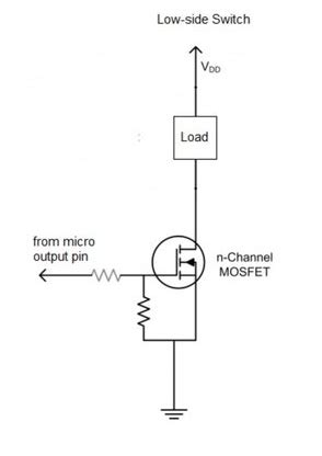
1. Gate Resistor
One of the simplest and most common techniques for MOSFET protection is the use of a gate resistor. By placing a resistor between the gate driver and the MOSFET gate, the rise time of the gate voltage is slowed down, reducing the risk of overshoot and ringing. The gate resistor also helps to limit the peak current during turn-on, reducing the stress on the MOSFET.
The value of the gate resistor should be carefully chosen based on the MOSFET characteristics and the desired switching speed. A higher resistance value provides better protection but may compromise the switching performance. It is important to strike a balance between protection and efficiency.
2. Zener Diode Clamp
Zener diodes can be used to clamp the gate voltage and protect against overvoltage conditions. By connecting a Zener diode between the gate and source of the MOSFET, the gate voltage is limited to the Zener breakdown voltage. If the gate voltage exceeds this threshold, the Zener diode conducts and shunts the excess voltage away from the gate.
The Zener diode should be chosen with a breakdown voltage slightly higher than the maximum allowable gate voltage of the MOSFET. It is important to ensure that the Zener diode can handle the expected current during the clamping action.
3. Transient Voltage Suppressor (TVS)
Transient Voltage Suppressors (TVS) are specialized devices designed to protect against voltage spikes and transients. TVS diodes have a fast response time and can clamp the voltage to a safe level within nanoseconds. They are commonly used to protect the gate and drain of MOSFETs from overvoltage events.
TVS diodes are connected in parallel with the MOSFET, typically between the gate and source or drain and source. When the voltage across the TVS exceeds its breakdown voltage, it enters avalanche breakdown mode and conducts, diverting the excess energy away from the MOSFET.
4. Snubber Circuit
Snubber circuits are used to suppress voltage spikes and ringing that can occur during MOSFET switching, particularly in inductive load applications. A snubber circuit typically consists of a resistor and a capacitor connected in series, placed across the drain and source of the MOSFET.
The snubber circuit absorbs the energy stored in the inductive load during turn-off, reducing the voltage spike across the MOSFET. The resistor value determines the damping effect, while the capacitor value determines the energy absorption capacity. Proper design of the snubber circuit is crucial to achieve effective protection without compromising switching performance.
5. Overtemperature Protection
To protect MOSFETs from thermal damage, overtemperature protection circuits can be implemented. These circuits monitor the temperature of the MOSFET and take protective action when a predefined temperature threshold is exceeded. Common overtemperature protection techniques include:
-
Thermistor-based protection: A thermistor with a negative temperature coefficient (NTC) is placed in close proximity to the MOSFET. As the temperature rises, the thermistor resistance decreases, triggering a protection circuit that can shut down the MOSFET or reduce its power dissipation.
-
Integrated temperature sensors: Some MOSFETs come with built-in temperature sensors that can be used to monitor the device temperature. These sensors provide an analog or digital output that can be used to implement overtemperature protection.
-
Thermal shutdown: In some cases, the MOSFET itself may have a thermal shutdown feature. When the junction temperature exceeds a certain threshold, the MOSFET automatically turns off to prevent thermal runaway and damage.
6. Electrostatic Discharge (ESD) Protection
ESD protection is crucial to prevent damage to MOSFETs during handling, assembly, and operation. The following techniques can be used to protect MOSFETs from ESD events:
-
ESD protection diodes: Specialized ESD protection diodes, such as transient voltage suppressor (TVS) diodes or Zener diodes, can be connected between the gate and source or drain and source of the MOSFET. These diodes clamp the voltage to a safe level during an ESD event, protecting the sensitive gate oxide.
-
Grounding and shielding: Proper grounding and shielding techniques can help dissipate static charges and prevent ESD events from reaching the MOSFET. This includes using grounded work surfaces, wrist straps, and ESD-safe packaging materials.
-
Design for ESD immunity: During the circuit design phase, techniques such as adding series resistors, using ESD-protected connectors, and implementing ESD-resistant PCB layouts can enhance the overall ESD immunity of the system.

MOSFET Protection Design Considerations
When designing MOSFET protection circuits, several key considerations should be taken into account to ensure optimal performance and reliability:
-
MOSFET characteristics: The protection techniques selected should be based on the specific characteristics of the MOSFET, including its voltage and current ratings, gate charge, and switching speed requirements.
-
Application requirements: The protection design should take into account the specific requirements of the application, such as the expected operating conditions, load characteristics, and performance targets.
-
Trade-offs: Implementing protection techniques often involves trade-offs between protection effectiveness, efficiency, and cost. It is important to strike a balance that meets the desired level of protection while minimizing the impact on overall system performance.
-
Simulation and testing: Proper simulation and testing are essential to validate the effectiveness of the protection design. This includes simulating various fault scenarios, conducting electrical tests, and performing environmental stress tests to ensure robust protection under different operating conditions.

Frequently Asked Questions (FAQ)
- What is the purpose of MOSFET protection?
-
MOSFET protection aims to safeguard MOSFETs from damage caused by overvoltage, overcurrent, electrostatic discharge (ESD), and high temperatures. By implementing appropriate protection techniques, the reliability and lifespan of MOSFETs can be significantly improved.
-
What are some common MOSFET protection techniques?
-
Some common MOSFET protection techniques include:
- Gate resistors to limit peak current and reduce overshoot and ringing.
- Zener diode clamps to protect against overvoltage conditions.
- Transient Voltage Suppressors (TVS) to suppress voltage spikes and transients.
- Snubber circuits to suppress voltage spikes and ringing during switching.
- Overtemperature protection circuits to prevent thermal damage.
- ESD protection diodes and proper grounding and shielding techniques.
-
How do I choose the appropriate protection technique for my MOSFET application?
-
The choice of protection technique depends on the specific requirements of your application and the characteristics of the MOSFET being used. Consider factors such as the expected operating conditions, load characteristics, and performance targets. It is recommended to consult the MOSFET datasheet and application notes for guidance on selecting suitable protection methods.
-
Can implementing MOSFET protection affect the overall system performance?
-
Yes, implementing MOSFET protection can sometimes involve trade-offs between protection effectiveness, efficiency, and cost. For example, adding a gate resistor may slow down the switching speed, while using a snubber circuit may increase power dissipation. It is important to carefully evaluate these trade-offs and strike a balance that meets the desired level of protection while minimizing the impact on system performance.
-
How can I validate the effectiveness of my MOSFET protection design?
- Validating the effectiveness of your MOSFET protection design involves thorough simulation and testing. Perform simulations to analyze the behavior of the protection circuits under various fault scenarios. Conduct electrical tests to verify the functionality and performance of the protection components. Additionally, perform environmental stress tests, such as temperature cycling and ESD testing, to ensure robust protection under different operating conditions.
Conclusion
MOSFET protection is essential to ensure the reliable operation and longevity of these critical components in electronic systems. By understanding the vulnerabilities of MOSFETs and implementing appropriate protection techniques, designers can effectively mitigate the risks associated with overvoltage, overcurrent, ESD, and high temperatures.
This article has explored various MOSFET protection methods, including gate resistors, Zener diode clamps, transient voltage suppressors, snubber circuits, overtemperature protection, and ESD protection techniques. Each technique has its own advantages and considerations, and the choice of protection method depends on the specific requirements of the application and the characteristics of the MOSFET.
When designing MOSFET protection circuits, it is crucial to consider factors such as MOSFET characteristics, application requirements, trade-offs, and proper simulation and testing. By following best practices and carefully evaluating the protection design, engineers can ensure robust and reliable MOSFET operation in a wide range of electronic applications.
Remember, investing in MOSFET protection not only safeguards the individual components but also contributes to the overall reliability and performance of the entire electronic system. By taking proactive measures to protect MOSFETs, designers can minimize the risk of failures, reduce maintenance costs, and enhance the long-term viability of their products.
As technology continues to advance and the demand for high-performance electronic systems grows, the importance of effective MOSFET protection becomes increasingly evident. By staying informed about the latest protection techniques and design practices, engineers can stay ahead of the curve and deliver robust and reliable solutions that meet the evolving needs of the industry.
No responses yet