Introduction to PCB Copper Layers
Printed Circuit Boards (PCBs) are essential components in modern electronics. They provide a platform for mounting and interconnecting electronic components to create functional circuits. One of the key elements of a PCB is the copper layer, which plays a crucial role in the board’s performance and functionality. In this article, we will explore PCB copper layers in-depth, discussing their types, manufacturing process, design considerations, and more.
What are Copper Layers in PCBs?
Copper layers in PCBs are thin sheets of copper foil laminated onto a non-conductive substrate material, typically fiberglass. These layers serve as conductive pathways for electrical signals and power distribution throughout the circuit board. The number of copper layers in a PCB can vary from one to multi-layer, depending on the complexity and requirements of the circuit design.
Why are Copper Layers Important in PCBs?
Copper layers play a vital role in PCBs for several reasons:
-
Electrical Conductivity: Copper is an excellent electrical conductor, allowing signals and power to flow efficiently through the circuit board.
-
Signal Integrity: Well-designed copper layers minimize signal interference, crosstalk, and impedance mismatch, ensuring reliable signal transmission.
-
Power Distribution: Copper layers provide low-resistance paths for power distribution, reducing voltage drops and ensuring stable power delivery to components.
-
Heat Dissipation: Copper’s thermal conductivity helps dissipate heat generated by electronic components, preventing overheating and improving the board’s reliability.
Types of PCB Copper Layers
PCBs can have different numbers and configurations of copper layers, depending on the circuit’s complexity and performance requirements. Let’s explore the common types of PCB copper layers.
Single-layer PCBs
Single-layer PCBs, also known as Single-Sided PCBs, have copper on only one side of the substrate. These boards are the simplest and most cost-effective option for basic circuits. Components are placed on the non-copper side of the board, and connections are made through holes drilled in the board and plated with copper.
Double-Layer PCBs
Double-layer PCBs, or double-sided PCBs, have copper layers on both sides of the substrate. This configuration allows for more complex circuit designs and higher component density compared to single-layer boards. Connections between the two layers are made using plated through-holes (PTHs) or vias.
Multi-Layer PCBs
Multi-layer PCBs consist of three or more copper layers sandwiched between insulating layers. These boards offer the highest level of complexity and density, enabling the routing of intricate circuits with numerous components. The inner layers are typically used for power and ground planes, while the outer layers are used for signal routing.
Here’s a table summarizing the different types of PCB copper layers:
| PCB Type | Copper Layers | Complexity | Cost |
|---|---|---|---|
| Single-Layer | 1 | Low | Low |
| Double-Layer | 2 | Medium | Medium |
| Multi-Layer | 3 or more | High | High |
PCB Copper Layer Manufacturing Process
The manufacturing process for PCB copper layers involves several steps to ensure the desired quality and functionality. Let’s take a closer look at each stage of the process.
Substrate Preparation
The first step in PCB manufacturing is preparing the substrate material, usually a fiberglass-reinforced epoxy resin known as FR-4. The substrate is cut to the desired size and shape, and any necessary holes are drilled for through-hole components or vias.
Copper Foil Lamination
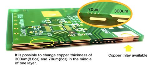
Next, thin sheets of copper foil are laminated onto the substrate using heat and pressure. The copper foil thickness is typically measured in ounces per square foot (oz/ft²), with common thicknesses being 0.5 oz, 1 oz, and 2 oz. The lamination process ensures a strong bond between the copper and the substrate.
Patterning and Etching
After lamination, the desired circuit pattern is transferred onto the copper layer using a photolithographic process. A photoresist layer is applied to the copper surface and exposed to UV light through a photomask containing the circuit pattern. The exposed areas of the photoresist are then developed and removed, leaving the copper exposed.
The exposed copper is etched away using a chemical solution, typically ferric chloride or ammonium persulfate. This process removes the unwanted copper, leaving only the desired circuit pattern on the substrate.
Plating and Finishing
After etching, the PCB undergoes additional plating and finishing processes to improve its performance and durability. These processes may include:
- Electroless copper plating: A thin layer of copper is deposited onto the exposed copper surfaces to improve adhesion and conductivity.
- Electrolytic copper plating: A thicker layer of copper is electroplated onto the board to increase the thickness of the copper traces and improve current-carrying capacity.
- Solder mask application: A protective layer of polymer is applied over the copper traces, leaving only the exposed pads and holes for component soldering.
- Surface finish application: A final finish, such as HASL (Hot Air Solder Leveling), ENIG (Electroless Nickel Immersion Gold), or OSP (Organic Solderability Preservative), is applied to the exposed copper surfaces to improve solderability and protect against oxidation.

PCB Copper Layer Design Considerations
Designing PCB copper layers requires careful consideration of various factors to ensure optimal performance and manufacturability. Here are some key design considerations:
Trace Width and Spacing
The width and spacing of copper traces on the PCB are critical factors in signal integrity and manufacturability. Trace width determines the current-carrying capacity and resistance of the trace, while spacing affects the potential for crosstalk and electromagnetic interference (EMI).
Designers must follow the manufacturer’s design rules and guidelines to ensure the traces are wide enough to carry the required current and spaced sufficiently apart to minimize interference. The table below shows typical trace width and spacing values for different copper thicknesses:
| Copper Thickness (oz/ft²) | Minimum Trace Width (mm) | Minimum Trace Spacing (mm) |
|---|---|---|
| 0.5 | 0.15 | 0.15 |
| 1 | 0.20 | 0.20 |
| 2 | 0.30 | 0.30 |
Power and Ground Planes
In multi-layer PCBs, dedicated power and ground planes are often used to provide low-impedance paths for power distribution and reduce noise. These planes are typically solid copper layers that cover most of the board area, with openings for signal vias and component pads.
Power and ground planes help maintain signal integrity by providing a stable reference voltage and minimizing voltage drops across the board. They also help reduce EMI by acting as shields between signal layers.
Via Design and Placement
Vias are conductive holes that allow signals to pass between different layers of the PCB. Proper via design and placement are crucial for maintaining signal integrity and manufacturability.
Designers must consider factors such as via size, drill diameter, and pad diameter to ensure reliable connections and prevent manufacturing issues. Additionally, the placement of vias should be optimized to minimize signal length and avoid interference with other components or traces.
Impedance Control
Impedance control is essential for high-speed digital circuits and RF applications. It involves designing the PCB copper layers to maintain a consistent characteristic impedance along the signal path, minimizing reflections and signal distortion.
Impedance control is achieved by carefully selecting the dielectric material, copper thickness, trace width, and spacing. Specialized software tools are often used to simulate and optimize the impedance of the PCB design.
PCB Copper Layer Testing and Inspection
After manufacturing, PCB copper layers must undergo thorough testing and inspection to ensure they meet the required quality standards and specifications. Some common testing and inspection methods include:
Visual Inspection
Visual inspection is the first step in PCB Quality control. Inspectors check for visible defects such as scratches, dents, or discoloration on the copper surface. They also verify the presence and accuracy of markings, such as part numbers and polarity indicators.
Automated Optical Inspection (AOI)
AOI uses high-resolution cameras and image processing algorithms to automatically detect and classify defects on the PCB surface. This method is particularly useful for identifying problems such as missing components, incorrect component placement, or solder bridging.
Electrical Testing
Electrical testing verifies the continuity and isolation of the copper traces and ensures the board functions as intended. Various test methods are used, including:
- Flying probe testing: A set of movable probes contacts specific points on the PCB to check for continuity, short circuits, and open circuits.
- In-circuit testing (ICT): The PCB is placed in a bed-of-nails fixture that makes contact with the board’s test points, allowing for comprehensive testing of components and interconnections.
- Functional testing: The assembled PCB is powered up and subjected to a series of operational tests to verify its performance under real-world conditions.
Microsectioning
Microsectioning is a destructive testing method that involves cutting a small cross-section of the PCB and examining it under a microscope. This technique is used to assess the quality of the copper plating, lamination, and via formation, as well as to measure the thickness of the copper layers and dielectric materials.
Frequently Asked Questions (FAQ)
-
What is the purpose of copper layers in PCBs?
Copper layers in PCBs serve as conductive pathways for electrical signals and power distribution. They allow components to be interconnected and enable the circuit to function as designed. -
How does the number of copper layers affect PCB performance?
Increasing the number of copper layers in a PCB allows for more complex circuit designs, higher component density, and better signal integrity. Multi-layer boards can dedicate layers to power and ground planes, reducing noise and improving power distribution. -
What factors determine the thickness of copper layers in PCBs?
The thickness of copper layers in PCBs is determined by the current-carrying requirements of the circuit, the desired impedance, and the manufacturing capabilities of the PCB fabricator. Common copper thicknesses include 0.5 oz, 1 oz, and 2 oz per square foot. -
How are PCB copper layers manufactured?
PCB copper layers are manufactured through a process that involves substrate preparation, copper foil lamination, patterning and etching, and plating and finishing. The desired circuit pattern is transferred onto the copper layer using photolithography, and unwanted copper is removed through etching. -
What are some key design considerations for PCB copper layers?
Key design considerations for PCB copper layers include trace width and spacing, power and ground plane design, via design and placement, and impedance control. Designers must follow manufacturer guidelines and use specialized tools to ensure optimal performance and manufacturability.
Conclusion
PCB copper layers are vital components in modern electronics, providing the conductive pathways necessary for signal transmission and power distribution. Understanding the types, manufacturing process, and design considerations of PCB copper layers is essential for creating high-quality, reliable circuit boards.
As PCB technology continues to advance, designers and manufacturers must stay up-to-date with the latest techniques and best practices for copper layer design and fabrication. By carefully considering factors such as trace width, spacing, impedance control, and testing methods, PCB designers can create boards that meet the ever-increasing demands of modern electronic devices.

No responses yet