What are PCB Layers?
PCB layers refer to the different levels or planes within a printed circuit board that are used to route signals and power between components. A PCB can have anywhere from one to over sixteen layers, depending on the complexity of the design and the requirements of the application.
Each layer in a PCB serves a specific purpose, such as:
- Providing a conductive path for signals
- Distributing power to components
- Acting as a ground plane to reduce noise and improve signal integrity
- Providing shielding to reduce electromagnetic interference (EMI)
The number of layers in a PCB is determined by the designer based on factors such as:
- The number of components and their placement
- The required signal routing density
- The power distribution requirements
- The need for shielding or noise reduction
- The manufacturing capabilities of the PCB fabricator
Types of PCB Layers
There are several types of layers that can be used in a PCB design, each with its own specific function. The most common types of PCB layers include:
Signal Layers
Signal layers are used to route electrical signals between components on the PCB. These layers are typically made of copper and are etched with the necessary conductive traces to connect the components. The number of signal layers in a PCB depends on the complexity of the design and the number of components that need to be connected.
Power Layers
Power layers are used to distribute power to the components on the PCB. These layers are typically made of copper and are designed to have a low resistance to minimize voltage drop and power loss. Power layers are usually placed near the center of the PCB stack-up to provide a low-impedance path for power distribution.
Ground Layers
Ground layers are used to provide a reference plane for the signals on the PCB and to reduce noise and improve signal integrity. These layers are typically made of copper and are connected to the ground pins of the components. Ground layers are usually placed adjacent to signal layers to provide a short return path for the signals and to minimize the loop area of the signal path.
Dielectric Layers
Dielectric layers are used to insulate the conductive layers in the PCB and to provide mechanical support. These layers are typically made of materials such as FR-4, which is a glass-reinforced epoxy laminate. The thickness of the dielectric layers depends on the required electrical and mechanical properties of the PCB.
Soldermask Layers
Soldermask layers are used to protect the copper traces on the PCB from oxidation and to prevent solder bridges from forming during the assembly process. These layers are typically made of a polymer material that is applied over the copper traces and then cured. The color of the soldermask layer can be customized to meet the aesthetic requirements of the application.
Silkscreen Layers
Silkscreen layers are used to add text and graphics to the PCB for identification and assembly purposes. These layers are typically made of a polymer material that is applied over the soldermask layer and then cured. The color of the silkscreen layer can be customized to meet the aesthetic requirements of the application.
PCB Layer Stack-up
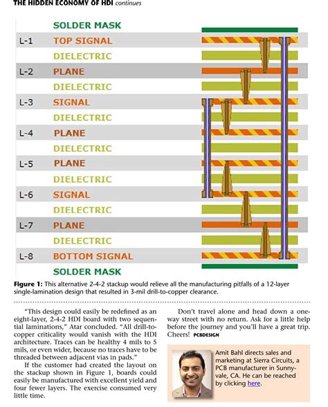
The arrangement of the different layers in a PCB is known as the layer stack-up. The stack-up is an important aspect of PCB design as it determines the electrical and mechanical properties of the board. The stack-up also affects the manufacturability and cost of the PCB.
A typical 4-layer PCB stack-up might look like this:
| Layer | Material | Thickness (mm) |
|---|---|---|
| Top Copper | Copper | 0.035 |
| Dielectric 1 | FR-4 | 0.2 |
| Inner Layer 1 (Ground) | Copper | 0.035 |
| Dielectric 2 | FR-4 | 0.7 |
| Inner Layer 2 (Power) | Copper | 0.035 |
| Dielectric 3 | FR-4 | 0.2 |
| Bottom Copper | Copper | 0.035 |
In this example, the top and bottom layers are used for signal routing, while the inner layers are used for power and ground distribution. The dielectric layers provide insulation and mechanical support.

Designing with PCB Layers
When designing a PCB, it is important to consider the number and arrangement of layers based on the requirements of the application. Here are some key considerations:
Signal Integrity
Signal integrity is critical in high-speed digital designs. To maintain signal integrity, it is important to use a sufficient number of signal layers and to route the signals carefully to minimize crosstalk and reflections. Ground planes should be used adjacent to signal layers to provide a low-impedance return path for the signals.
Power Distribution
Power distribution is another critical aspect of PCB design. To minimize voltage drop and power loss, it is important to use a sufficient number of power layers and to design the power distribution network carefully. The power layers should be placed near the center of the stack-up to minimize the impedance of the power distribution network.
EMI and Noise Reduction
Electromagnetic interference (EMI) and noise can be a significant problem in high-speed digital designs. To reduce EMI and noise, it is important to use shielding layers and to route signals carefully to minimize loop areas. Ground planes can also be used to provide a low-impedance path for noise currents.
Manufacturing Considerations
The number and arrangement of layers in a PCB also affects the manufacturability and cost of the board. In general, more layers means higher cost and longer manufacturing time. It is important to work with the PCB fabricator to ensure that the design is manufacturable and to optimize the stack-up for cost and performance.
FAQ
How many layers does a typical PCB have?
The number of layers in a PCB can vary widely depending on the complexity of the design and the requirements of the application. A simple single-sided PCB may have only one layer, while a complex Multilayer PCB can have sixteen or more layers. Most common PCBs have between two and eight layers.
What is the difference between a signal layer and a power layer?
Signal layers are used to route electrical signals between components on the PCB, while power layers are used to distribute power to the components. Signal layers are typically thinner and have more complex routing, while power layers are thicker and have simpler routing to minimize voltage drop and power loss.
What materials are used for PCB layers?
The most common material used for PCB layers is copper, which is an excellent conductor of electricity. The dielectric layers that provide insulation and mechanical support are typically made of materials such as FR-4, which is a glass-reinforced epoxy laminate. Soldermask and silkscreen layers are typically made of polymer materials.
How does the number of layers affect the cost of a PCB?
In general, more layers means higher cost and longer manufacturing time. This is because each additional layer requires additional materials, processing steps, and testing. However, the cost impact of additional layers can be offset by the improved performance and functionality that they provide.
Can I change the number of layers in an existing PCB design?
Changing the number of layers in an existing PCB design can be challenging, as it may require significant changes to the routing and component placement. It is generally easier to add layers than to remove them, as removing layers can disrupt the existing routing. If you need to change the number of layers in an existing design, it is important to work closely with the PCB fabricator to ensure that the changes are feasible and to minimize the impact on the overall design.
Conclusion
PCB layers are a critical aspect of printed circuit board design, providing a way to route signals and power between components while minimizing noise and interference. By understanding the different types of PCB layers and how they are used in PCB design, engineers and designers can create high-performance, reliable, and cost-effective electronic products.
Whether you are designing a simple Single-layer PCB or a complex multilayer board, it is important to consider the number and arrangement of layers based on the specific requirements of your application. By working closely with your PCB fabricator and following best practices for signal integrity, power distribution, and noise reduction, you can ensure that your PCB design meets the highest standards of quality and performance.

No responses yet