Introduction to PCB Manufacturing
Printed Circuit Boards (PCBs) are the backbone of modern electronics. They are used in almost every electronic device, from smartphones and computers to industrial equipment and medical devices. PCB manufacturing is a complex process that involves several steps, each of which requires precision and attention to detail. In this article, we will take a detailed look at the PCB manufacturing process, from design to final assembly.
The PCB Manufacturing Process
Step 1: PCB Design
The first step in the PCB manufacturing process is the design phase. This is where the circuit diagram is created using specialized software such as Altium, Eagle, or KiCad. The designer must consider several factors when creating the circuit diagram, including:
- Component placement
- Signal integrity
- Power distribution
- Thermal management
- Manufacturability
Once the circuit diagram is complete, it is converted into a set of files that can be used by the PCB manufacturer. These files include:
- Gerber files: These are the primary files used by PCB manufacturers. They contain information about the copper layers, solder mask, silkscreen, and drill holes.
- Drill files: These files contain information about the location and size of the drill holes.
- Bill of Materials (BOM): This is a list of all the components that will be used on the PCB.
- Assembly drawings: These drawings show where each component should be placed on the PCB.
Step 2: PCB Fabrication
Once the design files have been created, they are sent to the PCB manufacturer for fabrication. The fabrication process involves several steps:
PCB Material Selection
The first step in PCB fabrication is to select the appropriate material for the PCB. The most common materials used for PCBs are:
- FR-4: This is a glass-reinforced epoxy laminate that is commonly used for PCBs. It has good electrical and mechanical properties and is relatively inexpensive.
- High-Tg FR-4: This is a variation of FR-4 that has a higher glass transition temperature (Tg). It is used in applications where the PCB will be subjected to high temperatures.
- Polyimide: This is a high-performance material that is used in applications where the PCB will be subjected to extreme temperatures or harsh environments.
- Aluminum: This is used in applications where the PCB needs to dissipate a lot of heat, such as in power electronics.
PCB Lamination
Once the PCB material has been selected, it is laminated with copper foil on one or both sides. The copper foil is typically 1 or 2 ounces per square foot (oz/ft²), which corresponds to a thickness of 35 or 70 microns, respectively. The lamination process involves applying heat and pressure to bond the copper foil to the PCB material.
PCB Drilling
After the PCB has been laminated, it is drilled to create the holes for the components and vias. The drilling process is typically done using a computer numerical control (CNC) machine that can drill holes with a diameter as small as 0.1 mm. The drill bits used for PCB drilling are made of tungsten carbide and can be changed automatically by the CNC machine.
PCB Plating
Once the PCB has been drilled, it is plated with copper to create the electrical connections between the layers. The plating process involves several steps:
- Desmear: This step removes any debris or smear from the drill holes to ensure good electrical conductivity.
- Electroless copper: A thin layer of copper is deposited onto the PCB using a chemical process.
- Electrolytic copper: A thicker layer of copper is deposited onto the PCB using an electrical process.
- Tin: A thin layer of tin is deposited onto the copper to prevent oxidation.
PCB Etching
After the PCB has been plated, the unwanted copper is removed using a process called etching. The etching process involves applying a photoresist layer to the PCB and exposing it to light through a photomask. The areas of the photoresist that are exposed to light become soluble and can be washed away, leaving the copper exposed. The exposed copper is then removed using an etchant solution, typically ferric chloride or ammonium persulfate.
PCB Solder Mask Application
Once the unwanted copper has been removed, a solder mask is applied to the PCB. The solder mask is a layer of polymer that covers the copper traces and protects them from oxidation and short circuits. The solder mask is typically green, but other colors are available. The solder mask is applied using a silkscreen process and then cured using UV light.
PCB Silkscreen Application
The final step in PCB fabrication is to apply the silkscreen. The silkscreen is a layer of ink that is used to print text and symbols onto the PCB. The silkscreen is typically white, but other colors are available. The silkscreen is applied using a silkscreen process and then cured using UV light.
Step 3: PCB Assembly
Once the PCB has been fabricated, it is ready for assembly. The assembly process involves several steps:
Solder Paste Application
The first step in PCB assembly is to apply solder paste to the pads where the components will be placed. Solder paste is a mixture of tiny solder balls and flux that helps the solder adhere to the pads. The solder paste is typically applied using a stencil and a squeegee.
Component Placement
After the solder paste has been applied, the components are placed onto the PCB using a pick-and-place machine. The pick-and-place machine uses a vacuum nozzle to pick up the components and place them onto the pads. The machine is programmed with the coordinates of each component and can place thousands of components per hour.
Reflow Soldering
Once the components have been placed, the PCB is placed in a reflow oven. The reflow oven heats the PCB to a specific temperature profile that melts the solder paste and forms a strong bond between the components and the pads. The temperature profile is carefully controlled to ensure that the components are not damaged by the heat.
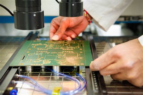
Inspection and Testing
After the PCB has been assembled, it is inspected and tested to ensure that it functions correctly. The inspection process typically involves a visual inspection to check for any obvious defects, such as missing components or solder bridges. The testing process involves using specialized equipment to test the functionality of the PCB, such as a flying probe tester or a boundary scan tester.

Advantages of PCB Manufacturing
PCB manufacturing offers several advantages over other methods of electronic assembly, such as point-to-point wiring or wire wrapping. Some of the advantages of PCB manufacturing include:
- Consistency: PCBs are manufactured using automated processes that ensure consistent quality and reliability.
- Compact size: PCBs allow electronic circuits to be packed into a small space, which is essential for modern electronic devices.
- High-speed: PCBs allow electronic signals to travel at high speeds, which is essential for high-performance electronic devices.
- Low cost: PCBs are relatively inexpensive to manufacture, especially in large quantities.
- Flexibility: PCBs can be designed to fit almost any shape or size, which allows for greater design flexibility.

Challenges in PCB Manufacturing
Despite the many advantages of PCB manufacturing, there are also several challenges that must be addressed. Some of the challenges in PCB manufacturing include:
- Miniaturization: As electronic devices become smaller and more complex, PCBs must also become smaller and more densely packed. This requires advanced manufacturing techniques and high-precision equipment.
- High-speed design: As electronic signals travel at higher speeds, PCBs must be designed to minimize signal integrity issues such as crosstalk and electromagnetic interference (EMI).
- Thermal management: As electronic components become more powerful, they generate more heat. PCBs must be designed to dissipate this heat effectively to prevent damage to the components.
- Environmental concerns: PCB manufacturing involves the use of hazardous chemicals and materials that can harm the environment if not disposed of properly. PCB manufacturers must follow strict environmental regulations to minimize their impact on the environment.

Conclusion
PCB manufacturing is a complex process that requires precision, attention to detail, and specialized equipment. The process involves several steps, from design to final assembly, each of which must be carefully controlled to ensure consistent quality and reliability. Despite the challenges involved in PCB manufacturing, it remains an essential technology for modern electronics. As electronic devices continue to become smaller, faster, and more complex, PCB manufacturing will continue to evolve to meet the demands of the industry.
FAQs
- What is the difference between a single-sided and double-sided PCB?
-
A single-sided PCB has copper traces on only one side of the board, while a double-sided PCB has copper traces on both sides of the board. Double-sided PCBs allow for more complex circuits and higher component density.
-
What is the purpose of the solder mask on a PCB?
-
The solder mask is a layer of polymer that covers the copper traces on a PCB. It serves two main purposes: to protect the copper from oxidation and to prevent solder bridges from forming between adjacent pads.
-
What is the difference between through-hole and surface-mount components?
-
Through-hole components have leads that are inserted into holes drilled in the PCB and soldered on the opposite side. Surface-mount components are placed directly onto pads on the surface of the PCB and soldered in place. Surface-mount components are smaller and allow for higher component density, but they require more precise placement and soldering.
-
What is the purpose of a reflow oven in PCB assembly?
-
A reflow oven is used to melt the solder paste and form a strong bond between the components and the pads on the PCB. The reflow oven heats the PCB to a specific temperature profile that is carefully controlled to ensure that the components are not damaged by the heat.
-
What are some common methods for testing PCBs?
- There are several common methods for testing PCBs, including:
- Visual inspection: Checking for obvious defects such as missing components or solder bridges
- Flying probe testing: Using a set of probes to test the connectivity and functionality of individual components and traces
- Boundary scan testing: Using a specialized test circuit to test the functionality of the PCB as a whole
- Functional testing: Testing the PCB in its intended application to ensure that it meets the required specifications.
No responses yet