Introduction to PCB Soldering
Printed Circuit Board (PCB) soldering is the process of joining electronic components to a PCB using molten metal solder. Soldering creates electrical and mechanical connections between component leads/pins and the copper pads on the PCB. Proper soldering techniques are critical for the reliability and functionality of electronic assemblies.
There are several different PCB soldering methods used in electronics manufacturing:
| Soldering Method | Description | Typical Applications |
|---|---|---|
| Hand Soldering | Manual soldering using a soldering iron | Prototypes, repairs, low-volume production |
| Wave Soldering | Components are passed over a molten wave of solder | Through-hole components, high-volume production |
| Reflow Soldering | Solder paste is applied and reflowed in an oven | Surface mount components, high-volume production |
| Selective Soldering | Precision soldering of specific areas | Mixed through-hole and SMD boards |
The choice of soldering technique depends on factors like the components used (through-hole vs surface mount), production volume, available equipment, and the specific application requirements.
Tools and Materials for PCB Soldering
To perform quality PCB soldering, it’s important to use the right tools and materials:
Soldering Iron
A soldering iron is the fundamental tool for hand soldering. Key considerations when selecting a soldering iron include:
- Wattage: Higher wattage irons heat up faster and maintain temperature better. 40-60W is suitable for most PCB work.
- Temperature Control: Adjustable temperature irons allow optimization for different Solder Types and components.
- Tip Style: Different tip shapes are used for different types of soldering. Conical and chisel tips are most common for PCB work.
Soldering Iron Tips
Using the right soldering iron tip is important for good results. Tips wear out over time and need to be replaced regularly.
| Tip Style | Characteristics | Uses |
|---|---|---|
| Conical | Pointed tip, good for precision | Tight spaces, SMD work |
| Chisel | Flat tip, good heat transfer | Drag soldering, larger joints |
| Bevel | Angled flat tip | Reaching joints at an angle |
Tips should be kept clean and well-tinned with solder for optimal heat transfer. Proper tip care helps extend tip life.
Solder
Solder is an alloy, typically consisting of tin and lead. Lead-free solder alloys are now widely used due to regulations restricting lead.
Important properties of solder include:
- Alloy Composition: Determines melting point, strength, and wetting properties. Common lead-free alloys include SAC305 (Sn96.5/Ag3.0/Cu0.5) and Sn99.3/Cu0.7.
- Solder Diameter: Varies from around 0.25mm to over 1mm. Smaller diameters are used for fine pitch components while larger are better for larger joints and hole filling.
- Flux Core: Rosin flux cores help the solder flow and make good joints. Flux types vary in activity from no-clean to water-soluble.
Solder is available in both wire and paste forms. Solder wire is used for hand soldering, while solder paste is used for reflow soldering.
Flux
Flux is a chemical agent that improves solder wetting and flow by removing oxides from metals. It is a key part of both solder wire and solder paste.
| Flux Type | Activity | Residue | Cleaning |
|---|---|---|---|
| Rosin | Mild | Non-corrosive | Optional |
| No-Clean | Mild | Minimal | Not required |
| Water-Soluble | High | Corrosive | Required |
The right flux type depends on the application, environment, and cleaning process. No-clean fluxes are very popular for PCB Assembly.
Other Tools & Accessories
- Tweezers for handling small components
- Solder wick for removing excess solder
- Flux pen for adding extra flux
- Fume extractor for removing harmful solder fumes
- Microscope or magnifier for inspecting joints

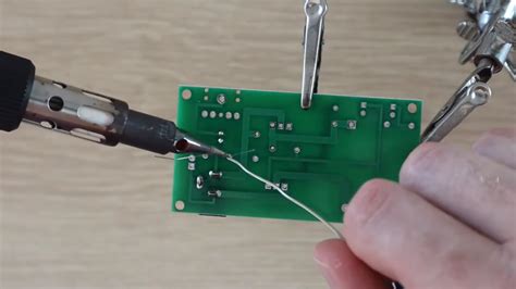
Hand Soldering Techniques
Hand soldering with a soldering iron remains a widely used technique for electronic assembly, rework, and repair. Mastering hand soldering takes practice to make consistent, reliable solder joints.
Tinning the Soldering Iron Tip
“Tinning” refers to coating the soldering iron tip with a layer of solder. This helps with heat transfer and protects the tip from oxidation.
To tin the tip:
- Set the iron to the right temperature for the solder type
- Clean the tip on a damp sponge or brass wool
- Apply a small amount of solder to the tip and let it melt, coating the tip
- Wipe off excess solder, leaving a thin, shiny coating
Re-tin the tip regularly to keep it in good condition and replace worn out tips.
Basic Soldering Steps
- Place the component into the PCB, bending the leads to hold it in place if needed
- Heat the pad and the lead simultaneously with the soldering iron
- Apply solder to the pad and lead, letting it melt and flow around the joint
- Remove the solder and then the iron, holding the component still until the joint cools
- Trim the excess lead with cutters
Key points to remember:
- Heat the joint, not the solder
- Use just enough solder to make a good joint
- Don’t move the joint until the solder solidifies
- Work quickly to avoid overheating components
Drag Soldering
Drag soldering is a technique for quickly soldering many pins, such as on connectors or IC chips.
- Flux and tin one row of pins
- Drag the iron tip along the row, melting the solder
- Repeat for the other side/row
Drag soldering takes practice to apply the right amount of solder and to avoid solder bridges between pins.
SMD Soldering
Soldering surface mount devices (SMDs) requires more precision than through-hole components due to their small size.
For small two-pin components like resistors and capacitors:
- Apply a small amount of solder to one pad
- Place the component with tweezers while heating the solder
- Solder the other side of the component
For chips and other multi-pin SMDs, drag soldering and solder wick are often used:
- Flux and tin one row of pins
- Drag solder along the row
- Use solder wick to remove bridges between pins
A fine tipped or hoof tipped iron is best for SMD soldering. Practice and good tools are key.

Reflow Soldering
Reflow soldering is the most common method for surface mount assembly, where components are attached to pads with solder paste and then heated to melt the solder.
Solder Paste
Solder paste is a suspension of fine solder powder in flux. It is applied to the PCB pads prior to placing components.
Solder pastes are characterized by:
- Alloy type
- Particle size and shape
- Flux type and activity
- Viscosity and slump
The right paste depends on the components, PCB finish, and reflow profile. Fine pitch components require fine particle pastes. Using a no-clean paste avoids the cleaning step.
Applying Paste
Solder paste is typically applied by printing through a patterned stencil onto the PCB pads.
Key factors in paste printing are:
- Stencil thickness and aperture size
- Squeegee pressure and speed
- Paste viscosity and rheology
- PCB and stencil alignment
Automated stencil printers give the most consistent results, but manual methods using a squeegee can work for prototypes and small runs.
After printing, a solder paste inspection (SPI) machine may be used to check the paste deposits for defects before placing components.
Pick and Place
After paste printing, the components are placed onto the PCB. For high volume production, this is done by automated pick and place (P&P) machines.
P&P machines use vacuum nozzles to pick up components from feeders or trays and place them precisely onto their pads on the PCB. They are programmed with the component locations and orientations.
For prototypes and small runs, components can be placed by hand using tweezers, though this is much slower and less precise than a machine.
Reflow Soldering Profile
After component placement, the PCB is passed through a reflow oven, which heats it according to a controlled temperature profile to melt the solder and form the joints.
A typical reflow profile has several stages:
- Preheat: The board is slowly heated to activate the flux and dry the paste
- Soak/Activation: The temperature is held steady to fully activate the flux
- Reflow: The temperature is raised above the solder melting point to let the solder melt and wet the surfaces
- Cooling: The board is cooled in a controlled way to let the solder solidify without defects
The exact temperatures and times of each stage depend on the solder paste, components, and PCB design. Following the paste manufacturer’s recommended profile is a good starting point.
Proper profiling and oven setup is crucial to get good reflow results without damaging the components or PCB.

Wave Soldering
Wave soldering is a common method for soldering through-hole components, where the PCB is passed over a wave of molten solder to coat the component pins.
Fluxing
Before wave soldering, the bottom of the PCB is coated with flux to clean and prepare the surfaces for soldering. This can be done by spraying or foaming the flux onto the board.
The flux type must be compatible with the solder alloy and the cleaning process. More active fluxes give better wetting but leave more residue.
Preheating
After fluxing, the PCB is preheated to activate the flux and dry out any solvents. Preheating also reduces thermal shock when the board hits the solder wave.
The preheater temperature and time depends on the flux type, solder, and board design. Typically the flux will be mostly dried out but not burnt at the end of preheat.
Solder Wave
The heart of the wave soldering machine is the solder pot and wave. The pot holds a large volume of molten solder, heated to around 260°C. The solder is pumped up through a nozzle to form a standing wave.
As the PCB passes over the wave, the bottom surface contacts the solder, coating the exposed pads and through-hole pins. The wave shape, height, and flow rate are adjusted to get good hole fill and coating without defects like bridging or icicles.
Dual wave machines use a turbulent wave followed by a smooth one to reduce defects. Some have additional features like air knives to control solder thickness.
Cooling
After the wave, the PCB cools and the solder solidifies in a controlled manner to form good joint fillets and avoid defects like cracks or voids. The conveyor angle and speed affect the cooling rate.
Some machines have a dedicated cooling zone with air knives or inert atmosphere. Gradual, even cooling is best for joint quality.
Cleaning
Depending on the flux type, cleaning may be required to remove flux residues after soldering.
Water soluble fluxes must be cleaned, typically in an inline aqueous cleaning machine. Rosin fluxes can be cleaned if cosmetics are important. No-clean fluxes generally don’t require cleaning.
The cleaning process and chemistry must be compatible with the flux and the PCB/component materials to avoid damage or reliability issues.
Inspection and Quality Control
Inspection is a critical part of the PCB assembly process to find and correct soldering defects before the product is shipped.
Visual Inspection
Visual inspection is the first line of quality control, catching obvious defects. It can be done manually by operators or with automated optical inspection (AOI) systems.
Some key things to look for:
- Missing or misaligned components
- Solder bridges or icicles
- Poor wetting or de-wetting
- Cracked or dull joints
- Insufficient or excessive solder
Visual standards like IPC-A-610 give criteria for acceptable solder joints. Inspection should be done under bright lighting and magnification.
X-Ray Inspection
X-ray inspection allows seeing inside solder joints to find hidden defects like voids, balls, or poor hole fill. It is especially useful for BGA and other area array packages where the joints are not visible.
X-ray systems use either 2D or 3D imaging to look at joint structure and measure voiding levels. Automated X-ray inspection (AXI) systems can check the whole PCB quickly.
Interpreting X-ray images takes training and experience to distinguish defects from normal variations. IPC-7095 and other standards give guidance on X-ray inspection criteria.
Electrical Test
Electrical testing verifies that the soldered assembly actually functions correctly and meets specifications. This can range from a simple continuity test to a full functional test.
In-circuit test (ICT) checks for short circuits, open circuits, and component values by probing test points on the PCB. Flying probe testers are often used for this.
Functional test applies power and signals to the PCB to verify that it operates as intended. This may involve custom test fixtures and software.
Boundary scan is another technique for Digital PCBs, using built-in test circuitry to check interconnects and logic.
Electrical test catches defects that may not be visible but could still cause field failures. It is an important final quality gate.
Soldering Defects and Troubleshooting
Despite our best efforts, soldering defects can still occur. Knowing how to recognize and troubleshoot common issues is key to improving the process.
Some typical soldering defects include:
| Defect | Appearance | Causes | Remedies |
|---|---|---|---|
| Solder Bridge | Solder connecting adjacent pins/pads | Excess solder, poor tip technique | Solder wick, better technique |
| Cold Joint | Dull, cracked, or lumpy joint | Insufficient heat, poor wetting | More flux, higher iron temp |
| Void | Bubble within the joint (seen by X-ray) | Moisture, contamination, rapid cooling | Better drying, slower cooling |
| Tombstone | Component lifted up on one end | Uneven heating, paste slump | Reduce paste volume, even heating |
| Icicle | Sharp spike of solder hanging down | Excess solder, slow solder solidification | Adjust wave parameters, faster cooling |
When troubleshooting soldering problems, a systematic approach is best:
- Identify the specific defect and its frequency
- Check the solder materials and PCB condition
- Review the process parameters and settings
- Examine the equipment condition and calibration
- Observe the operator technique or programming
- Make one change at a time and retest
- Document the findings and solution
Tools like cause-effect diagrams and design of experiments (DOE) can help pinpoint the root cause of soldering issues. Keeping careful process records is also valuable for tracking down problems.
In some cases, the PCB design itself may be the culprit, with issues like insufficient pad size, poor thermal relief, or difficult component placement. Design for manufacturability (DFM) guidelines help avoid these problems.
FAQ
Q1: What’s the difference between lead and lead-free solder?
A1: Leaded solder typically contains 63% tin and 37% lead, while lead-free solder replaces the lead with other metals like silver and copper. Lead-free solder has a higher melting point and can be more brittle than leaded. It is now widely used due to regulations restricting lead in electronics.
Q2: How hot should my soldering iron be?
A2: The ideal soldering iron temperature depends on the solder type and the job. A general range is 600-800°F (315-425°C). Lead-free solder usually requires higher temperatures than leaded. Start on the lower end and increase temperature if needed for good wetting. Too high a temperature can damage components and PCBs.
Q3: What’s the best way to remove solder bridges?
A3: Solder wick and a soldering iron is the most common method. Place the wick over the bridge and apply the iron to heat the wick and melt the solder, which will be drawn up into the wick. Flux can help the process. Solder suckers can also be used but may stress the PCB more.
Q4: How much paste should I apply for reflow?
A4: The solder paste volume depends on the pad size, stencil aperture, and solder joint requirements. A typical stencil thickness is 0.005″ to 0.008″ (0.125 to 0.2mm). The aperture size is usually close to the pad size. Too much paste can cause bridging while too little can lead to open joints. Following the paste and component supplier guidelines is a good start.
No responses yet