Understanding PCB Return Currents
In the world of PCB design, understanding and properly managing return currents is crucial for ensuring signal integrity and reducing electromagnetic interference (EMI). Return currents are the currents that flow back to the source, completing the electrical circuit. The path taken by these return currents can significantly impact the performance and reliability of a PCB. In this article, we will explore various return current topologies and their implications for PCB design.
What are Return Currents?
When a signal travels through a trace on a PCB, it generates a corresponding return current that flows back to the source. These return currents follow the path of least impedance, which is often the reference plane (ground or power plane) closest to the signal trace. The return current path is essential for maintaining signal integrity and minimizing EMI.
Importance of Return Current Management
Proper management of return currents is critical for several reasons:
-
Signal Integrity: Poorly managed return currents can lead to signal distortion, crosstalk, and increased noise, compromising the integrity of the transmitted signals.
-
EMI Reduction: Uncontrolled return currents can create unintended loops, acting as antennas and radiating electromagnetic energy, resulting in EMI issues.
-
Power Integrity: Improper return current paths can cause voltage drops and power supply noise, affecting the stability and performance of the PCB.
Return Current Topologies
There are several return current topologies commonly used in PCB design, each with its own characteristics and benefits. Let’s explore some of the most prevalent topologies.
1. Solid Ground Plane
A solid ground plane is the most common and preferred return current topology in PCB design. It involves dedicating an entire copper layer to serve as a low-impedance reference plane for the return currents. The solid ground plane provides a continuous and uninterrupted path for the return currents to flow back to the source.
Advantages:
– Provides a low-impedance path for return currents
– Minimizes loop areas and reduces EMI
– Helps maintain signal integrity
– Offers better shielding and noise suppression
Considerations:
– Requires dedicated copper layer(s)
– May increase PCB thickness and manufacturing cost
2. Gridded Ground Plane
A gridded ground plane is an alternative to a solid ground plane, where the reference plane is divided into a grid pattern. The grid is formed by creating a matrix of copper strips or squares connected at regular intervals. The signal traces are routed between the grid lines, and the return currents flow through the grid structure.
Advantages:
– Reduces copper usage compared to a solid ground plane
– Allows for better control of impedance
– Provides flexibility in routing signal traces
Considerations:
– Requires careful design to ensure adequate return current paths
– May introduce additional inductance and resistance
– Increases design complexity
3. Split Planes
Split planes involve dividing a reference plane into multiple sections, each serving a specific purpose or power domain. This topology is commonly used when different parts of the PCB require separate ground or power references. The split planes are typically connected through a common point, such as a star ground or a power distribution network.
Advantages:
– Allows for isolation between different sections of the PCB
– Helps prevent noise coupling between power domains
– Enables targeted return current management
Considerations:
– Requires careful planning and placement of split planes
– May introduce discontinuities in return current paths
– Needs proper stitching or coupling between split planes
4. Mixed-Signal Planes
Mixed-signal planes are used in PCBs that incorporate both analog and digital circuitry. In this topology, separate reference planes are used for analog and digital sections to minimize noise coupling and interference. The analog and digital ground planes are typically connected at a single point, known as a “star ground,” to prevent ground loops.
Advantages:
– Provides isolation between analog and digital sections
– Reduces noise coupling and interference
– Allows for optimized return current paths for each domain
Considerations:
– Requires careful placement of components and routing
– Needs proper separation and shielding between analog and digital sections
– May increase PCB complexity and layer count

Designing for Optimal Return Current Flow
To ensure optimal return current flow and minimize EMI, consider the following guidelines when designing your PCB:
- Place signal traces close to their respective reference planes to minimize loop areas.
- Use continuous and uninterrupted reference planes whenever possible.
- Avoid splitting reference planes unnecessarily, as it can create discontinuities in return current paths.
- Use stitching capacitors or vias to provide low-impedance connections between reference planes.
- Route high-speed signals over uninterrupted reference planes to maintain signal integrity.
- Minimize the use of slots or gaps in reference planes, as they can disrupt return current flow.
- Consider the use of shielding techniques, such as guard traces or ground pours, to contain return currents and reduce EMI.

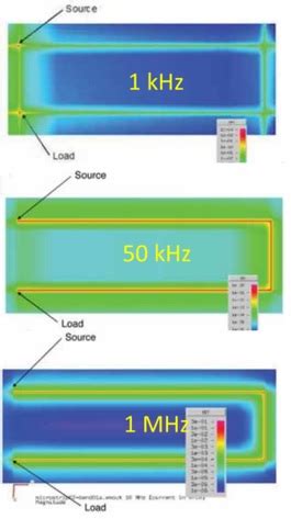
Analyzing Return Current Paths
To analyze and optimize return current paths in your PCB design, you can use various tools and techniques:
-
Current Density Simulation: Use electromagnetic simulation software to visualize and analyze the current density distribution on your PCB. This helps identify areas of high current concentration and potential bottlenecks.
-
Inductance Calculation: Calculate the loop inductance of your signal traces and return current paths. Minimizing loop inductance reduces EMI and improves signal integrity.
-
Impedance Control: Ensure that the impedance of your signal traces matches the impedance of the return current path. Impedance mismatch can lead to signal reflections and degradation.
-
Time-Domain Reflectometry (TDR): Use TDR measurements to identify discontinuities and impedance mismatches in your return current paths. TDR helps locate and resolve issues related to signal integrity.

Real-World Examples
Let’s look at a few real-world examples that demonstrate the importance of proper return current management in PCB design.
Example 1: High-Speed Digital PCB
In a high-speed digital PCB, such as a computer motherboard, the return current topology plays a crucial role in maintaining signal integrity and reducing EMI. A solid ground plane is often used as the primary return current path for the high-speed signals. The ground plane is placed close to the signal traces to minimize loop areas and provide a low-impedance return path.
Additionally, split planes may be used to isolate different power domains, such as the CPU, memory, and I/O sections. Stitching capacitors are placed between the split planes to provide a low-impedance connection and prevent ground bounce.
Example 2: Mixed-Signal PCB
In a mixed-signal PCB, such as an audio processing board, proper isolation between analog and digital sections is essential to minimize noise coupling. A mixed-signal plane topology is employed, where separate ground planes are used for the analog and digital domains.
The analog ground plane is kept clean and isolated from the digital ground plane to prevent digital noise from contaminating the sensitive analog signals. The analog and digital ground planes are connected at a single point, usually near the power supply, to prevent ground loops.
Example 3: RF PCB
In a radio frequency (RF) PCB, such as a wireless communication module, the return current topology is critical for maintaining signal integrity and minimizing EMI. A solid ground plane is often used as the primary return current path for the RF signals.
The ground plane is carefully designed to provide a continuous and uninterrupted path for the return currents. Stitching vias are used to connect the ground plane to the component ground pins, ensuring a low-impedance connection. Additionally, shielding techniques, such as ground pours and guard traces, are employed to contain the return currents and reduce EMI.
Frequently Asked Questions (FAQ)
-
Q: What is the difference between a solid ground plane and a gridded ground plane?
A: A solid ground plane is a continuous and uninterrupted copper layer that serves as a low-impedance reference plane for return currents. On the other hand, a gridded ground plane is divided into a grid pattern, with signal traces routed between the grid lines. Gridded ground planes offer more flexibility in routing but may introduce additional inductance and resistance compared to solid ground planes. -
Q: Why is it important to minimize loop areas in PCB design?
A: Minimizing loop areas in PCB design is crucial for reducing electromagnetic interference (EMI) and maintaining signal integrity. When a signal trace and its corresponding return current path form a loop, it acts as an antenna, radiating electromagnetic energy. By keeping the loop areas small, the amount of EMI generated is minimized, and the signal integrity is preserved. -
Q: What are split planes, and when are they used?
A: Split planes are reference planes that are divided into multiple sections, each serving a specific purpose or power domain. They are commonly used when different parts of the PCB require separate ground or power references. Split planes help isolate noise coupling between different sections of the PCB and enable targeted return current management. -
Q: How can I analyze and optimize return current paths in my PCB design?
A: To analyze and optimize return current paths, you can use various tools and techniques, such as current density simulation, inductance calculation, impedance control, and time-domain reflectometry (TDR). These methods help identify areas of high current concentration, minimize loop inductance, ensure impedance matching, and locate discontinuities in return current paths. -
Q: What are some guidelines for ensuring optimal return current flow in PCB design?
A: To ensure optimal return current flow, consider the following guidelines: - Place signal traces close to their respective reference planes.
- Use continuous and uninterrupted reference planes whenever possible.
- Avoid splitting reference planes unnecessarily.
- Use stitching capacitors or vias to provide low-impedance connections between reference planes.
- Route high-speed signals over uninterrupted reference planes.
- Minimize the use of slots or gaps in reference planes.
- Consider using shielding techniques, such as guard traces or ground pours.
Conclusion
Understanding and properly managing return currents is essential for achieving signal integrity, reducing EMI, and ensuring the overall performance and reliability of PCBs. By selecting the appropriate return current topology based on the specific requirements of your PCB, such as a solid ground plane, gridded ground plane, split planes, or mixed-signal planes, you can optimize the return current flow and minimize the impact of EMI.
Remember to follow best practices in PCB design, such as minimizing loop areas, using continuous reference planes, and employing shielding techniques when necessary. Additionally, utilizing tools and techniques like current density simulation, inductance calculation, and TDR can help you analyze and optimize return current paths effectively.
By paying close attention to return current management in your PCB designs, you can create robust and reliable electronic systems that meet the ever-increasing demands of today’s technology landscape.
No responses yet