Introduction to Solder Mask
Solder mask, also known as solder resist or solder stop mask, is a thin layer of polymer applied to the copper traces of a printed circuit board (PCB) to protect them from oxidation, prevent solder bridges, and provide electrical insulation. It is a crucial component in the manufacturing process of PCBs, as it ensures the reliability and longevity of the electronic device.
What is a Printed Circuit Board (PCB)?
A printed circuit board is a flat board made of insulating material, such as fiberglass or composite epoxy, with conductive copper traces etched onto its surface. These copper traces form the electrical connections between various components mounted on the board, such as resistors, capacitors, and integrated circuits. PCBs are the foundation of modern electronic devices, ranging from smartphones and laptops to industrial control systems and medical equipment.
The Role of Solder Mask in PCB Manufacturing
Solder mask plays a vital role in the PCB manufacturing process by:
- Protecting the copper traces from oxidation and corrosion
- Preventing solder bridges between adjacent traces during the soldering process
- Providing electrical insulation between conductive parts
- Improving the aesthetics of the PCB by giving it a uniform color (usually green, red, blue, or black)
- Facilitating the placement of component labels and other markings on the board
Types of Solder Mask
There are two main types of solder mask used in PCB manufacturing:
- Liquid Photoimageable Solder Mask (LPISM)
- Dry Film Photoimageable Solder Mask (DFPSM)
Liquid Photoimageable Solder Mask (LPISM)
LPISM is the most common type of solder mask used in the PCB industry. It is a liquid polymer that is applied to the PCB surface using screen printing, curtain coating, or spraying techniques. The liquid solder mask is then exposed to ultraviolet (UV) light through a photographic film, which hardens the exposed areas while leaving the unexposed areas soluble. The unexposed areas are then removed using a developer solution, revealing the copper pads and traces that need to be soldered.
Advantages of LPISM:
- Provides excellent conformity to the PCB surface
- Offers high resolution and fine pitch capability
- Allows for easy repair and rework
- Cost-effective for small to medium-sized production runs
Disadvantages of LPISM:
- Requires a longer processing time compared to DFPSM
- May have a slightly uneven surface finish
- Can be prone to pinholes and other defects if not applied properly
Dry Film Photoimageable Solder Mask (DFPSM)
DFPSM is a solid photopolymer film that is laminated onto the PCB surface using heat and pressure. Like LPISM, it is exposed to UV light through a photographic film, which crosslinks the exposed areas while leaving the unexposed areas soluble. The unexposed areas are then removed using a developer solution.
Advantages of DFPSM:
- Provides a uniform and consistent surface finish
- Offers excellent adhesion to the PCB surface
- Allows for faster processing times compared to LPISM
- Suitable for high-volume production runs
Disadvantages of DFPSM:
- Higher material cost compared to LPISM
- Less conformity to the PCB surface, which may cause issues with fine pitch components
- More difficult to repair and rework

Solder Mask Application Process
The solder mask application process typically involves the following steps:
-
Surface Preparation: The PCB surface is cleaned and roughened to ensure proper adhesion of the solder mask.
-
Solder Mask Application: The solder mask is applied to the PCB surface using screen printing, curtain coating, spraying (for LPISM), or lamination (for DFPSM).
-
Exposure: The solder mask is exposed to UV light through a photographic film, which crosslinks the exposed areas while leaving the unexposed areas soluble.
-
Developing: The unexposed areas of the solder mask are removed using a developer solution, revealing the copper pads and traces that need to be soldered.
-
Curing: The solder mask is cured using heat to fully crosslink the polymer and improve its mechanical and chemical properties.
-
Inspection: The PCB is inspected for any defects or imperfections in the solder mask, such as pinholes, bubbles, or misalignment.
Solder Mask Thickness
The thickness of the solder mask is an important factor in PCB manufacturing, as it affects the board’s electrical insulation, mechanical protection, and aesthetic appearance. The typical thickness of a solder mask ranges from 0.8 to 1.5 mils (20 to 38 microns), depending on the application and the type of solder mask used.
| Solder Mask Type | Typical Thickness Range (mils) | Typical Thickness Range (microns) |
|---|---|---|
| LPISM | 0.8 – 1.2 | 20 – 30 |
| DFPSM | 1.0 – 1.5 | 25 – 38 |
Thicker solder masks provide better insulation and protection but may cause issues with fine pitch components and high-density PCB designs. Thinner solder masks, on the other hand, offer better conformity and resolution but may be more prone to defects and damage.
Solder Mask Color
Solder mask is available in a variety of colors, with green being the most common. Other popular colors include red, blue, black, and white. The choice of solder mask color is usually based on aesthetic preferences, but it can also serve functional purposes, such as:
- Improving the contrast between the solder mask and the component markings for easier assembly and inspection
- Reducing the reflectivity of the PCB surface to minimize light interference in optical applications
- Enhancing the heat dissipation properties of the PCB by using lighter colors that reflect more heat

Solder Mask Performance Properties
A high-quality solder mask should exhibit the following performance properties:
-
Electrical Insulation: The solder mask should provide sufficient electrical insulation between conductive parts to prevent short circuits and leakage currents.
-
Chemical Resistance: The solder mask should be resistant to various chemicals used in the PCB manufacturing process, such as fluxes, solvents, and cleaning agents.
-
Thermal Stability: The solder mask should be able to withstand the high temperatures encountered during soldering and other thermal processes without degrading or delaminating.
-
Mechanical Strength: The solder mask should have good adhesion to the PCB surface and be resistant to scratches, abrasion, and impact.
-
Moisture Resistance: The solder mask should provide a barrier against moisture ingress, which can cause corrosion and degrade the electrical performance of the PCB.
-
Flammability Resistance: The solder mask should be flame-retardant to minimize the risk of fire in case of electrical faults or overheating.
Solder Mask Standards and Specifications
There are several industry standards and specifications that define the requirements for solder mask performance, such as:
- IPC-SM-840: Qualification and Performance Specification of Permanent Solder Mask
- IPC-4781: Qualification and Performance Specification of Permanent Coating (Liquid Coating) for Rigid Printed Circuit Boards
- MIL-PRF-55110: Military Specification for Printed Wiring Board, Rigid, General Specification for
These standards provide guidelines for testing and evaluating the electrical, mechanical, and chemical properties of solder masks, as well as their compatibility with various PCB manufacturing processes and end-use applications.

Solder Mask Design Considerations
When designing a PCB with solder mask, there are several factors to consider to ensure optimal performance and manufacturability:
-
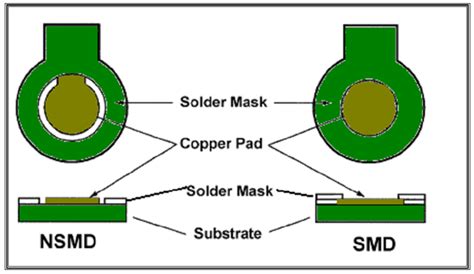
Solder Mask Clearance: The solder mask should have sufficient clearance around the copper pads and traces to allow for proper solder joint formation and prevent solder bridging. The typical solder mask clearance is 2 to 5 mils (50 to 125 microns) larger than the copper feature size.
-
Solder Mask Expansion: The solder mask may expand or contract during the curing process, which can cause misalignment with the copper features. Designers should account for this expansion by adding appropriate compensation factors to the solder mask artwork.
-
Solder Mask Registration: The solder mask should be accurately registered with the copper features to ensure proper insulation and protection. Misregistration can lead to exposed copper, solder bridging, or poor adhesion of the solder mask.
-
Solder Mask Sliver: A solder mask sliver is a thin strip of solder mask between two adjacent copper features. If the sliver is too narrow, it may break off during the manufacturing process or in the field, causing short circuits or other reliability issues. Designers should ensure that the solder mask slivers are wide enough to withstand the stresses of manufacturing and use.
-
Solder Mask Dambar: A solder mask dambar is a thin strip of solder mask that connects two adjacent copper pads to prevent solder bridging during the assembly process. The dambar is typically removed after soldering using a laser or mechanical process. Designers should ensure that the dambar is strong enough to withstand the soldering process but also easy to remove without damaging the PCB.
Solder Mask Design Tools and Software
There are various PCB design tools and software that can help designers create and optimize solder mask layouts, such as:
- Altium Designer
- Cadence Allegro PCB Designer
- Mentor Graphics PADS
- Zuken CR-8000
These tools provide features such as automatic solder mask generation, design rule checking (DRC), and 3D visualization to ensure that the solder mask design meets the required specifications and performance criteria.
Frequently Asked Questions (FAQ)
- What is the difference between solder mask and conformal coating?
-
Solder mask is applied to the PCB surface before the soldering process to protect the copper traces and prevent solder bridging. Conformal coating, on the other hand, is applied after the soldering process to provide additional protection against moisture, dust, and other environmental factors.
-
Can solder mask be removed for rework or repair?
-
Yes, solder mask can be removed using chemical or mechanical methods, such as solvents, abrasives, or lasers. However, the removal process should be carefully controlled to avoid damaging the underlying copper features or the PCB substrate.
-
What is the shelf life of solder mask?
-
The shelf life of solder mask depends on the specific product and storage conditions. Most liquid photoimageable solder masks have a shelf life of 6 to 12 months when stored at room temperature and protected from light. Dry film solder masks typically have a longer shelf life of 12 to 24 months under similar storage conditions.
-
How does solder mask affect the impedance of PCB Traces?
-
Solder mask has a dielectric constant that is higher than air, which can affect the impedance of PCB traces. Designers should take into account the thickness and dielectric constant of the solder mask when calculating the impedance of controlled impedance traces, such as those used in high-speed digital or RF applications.
-
Can solder mask be used on Flexible PCBs?
- Yes, solder mask can be applied to flexible PCBs using specialized materials and processes that can withstand the bending and flexing of the substrate. Flexible solder masks are typically made of polyimide or other flexible polymers and are applied using screen printing or photoimaging techniques.
Conclusion
Solder mask is a critical component in the PCB manufacturing process, providing essential protection, insulation, and aesthetic benefits to the final product. By understanding the types, properties, and design considerations of solder mask, PCB designers and manufacturers can ensure the reliability, performance, and longevity of their electronic devices.
As PCB technology continues to evolve, with increasing demands for higher density, faster speeds, and greater functionality, the role of solder mask will become even more important in enabling these advancements. Ongoing research and development in solder mask materials, processes, and design tools will be crucial in meeting the challenges and opportunities of the future PCB industry.
No responses yet