What is BGA?
BGA, or Ball Grid Array, is a type of surface-mount packaging used for integrated circuits (ICs) that utilizes a grid of solder balls as the means of interconnection between the IC and the printed circuit board (PCB). This packaging technology has gained significant popularity in recent years due to its numerous advantages over traditional packaging methods, such as higher pin density, better thermal and electrical performance, and smaller package size.
Advantages of BGA Packaging
- High pin density: BGA packages can accommodate a large number of interconnections in a small area, making them ideal for complex, high-performance ICs.
- Improved thermal performance: The solder balls in BGA packages provide a low-resistance thermal path, allowing for better heat dissipation compared to other packaging types.
- Enhanced electrical performance: The short, uniform length of the solder balls minimizes signal distortion and provides better signal integrity.
- Smaller package size: BGA packages have a smaller footprint compared to other packaging types with the same pin count, enabling more compact PCB designs.
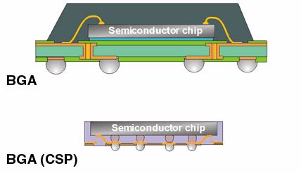
BGA Package Structure
A typical BGA package consists of the following components:
- IC die: The semiconductor chip that performs the desired functions.
- Substrate: A laminated material, usually made of bismaleimide triazine (BT) resin or polyimide, that provides mechanical support and electrical connections between the die and the solder balls.
- Wire bonds or flip-chip interconnects: The electrical connections between the die and the substrate. Wire bonding uses thin gold or copper wires, while flip-chip interconnects use solder bumps.
- Solder balls: The spherical solder balls that form the electrical and mechanical connection between the package and the PCB.
- Encapsulant: A protective material, typically epoxy-based, that covers and protects the die and wire bonds.
BGA Package Types
There are several types of BGA packages, each with its own unique features and applications:
| BGA Package Type | Description | Applications |
|---|---|---|
| Plastic BGA (PBGA) | Uses a plastic substrate and wire bonding | Consumer electronics, mobile devices |
| Ceramic BGA (CBGA) | Uses a ceramic substrate for higher reliability | Military, aerospace, high-temperature applications |
| Tape BGA (TBGA) | Uses a flexible tape substrate for thinner packages | Mobile devices, wearables |
| Flip-Chip BGA (FCBGA) | Uses flip-chip interconnects instead of wire bonding | High-performance computing, gaming consoles |

BGA PCB Design Considerations
Designing a PCB for BGA packages requires careful consideration of several factors to ensure optimal performance and reliability:
1. Pad Size and Pitch
The pad size and pitch (distance between the centers of adjacent pads) must match the solder ball size and pitch of the BGA package. Common BGA pitches range from 0.5mm to 1.27mm, with solder ball diameters ranging from 0.25mm to 0.6mm.
2. PCB Stack-up
The PCB stack-up should be designed to minimize signal integrity issues and provide adequate power and ground planes. A typical BGA PCB stack-up may include:
- Top and bottom signal layers
- Power and ground planes
- Inner signal layers
- Dielectric layers
3. Via Types and Placement
Vias are used to connect the BGA pads to the inner layers of the PCB. There are several types of vias used in BGA PCB design:
| Via Type | Description |
|---|---|
| Through-hole vias | Extend through the entire thickness of the PCB |
| Blind vias | Extend from the surface to an inner layer |
| Buried vias | Connect inner layers without extending to the surface |
| Microvias | Small-diameter vias used for high-density interconnects |
Via placement should be optimized to minimize signal integrity issues and avoid solder ball interference during assembly.
4. Thermal Management
Proper thermal management is crucial for BGA PCBs to prevent overheating and ensure long-term reliability. Thermal management strategies include:
- Using thermal vias to transfer heat from the BGA package to the PCB
- Incorporating thermal planes or heatsinks
- Selecting PCB materials with appropriate thermal conductivity
5. Signal Integrity
Signal integrity is a critical consideration in BGA PCB design, especially for high-speed applications. Signal integrity issues can be addressed by:
- Minimizing trace lengths and impedance discontinuities
- Using controlled impedance traces and differential pairs
- Implementing proper grounding and shielding techniques

BGA Assembly Process
The BGA assembly process involves several steps to ensure proper attachment of the BGA package to the PCB:
- Solder paste application: Solder paste is applied to the BGA pads on the PCB using a stencil or screen printing process.
- Package placement: The BGA package is precisely placed on the PCB using pick-and-place equipment, aligning the solder balls with the corresponding pads.
- Reflow soldering: The PCB Assembly is heated in a reflow oven, causing the solder paste to melt and form a permanent connection between the solder balls and the pads.
- Inspection: The assembLED PCB is inspected using X-ray or automated optical inspection (AOI) equipment to verify proper solder joint formation and detect any defects.
BGA Rework and Repair
In case of defects or failures, BGA packages may need to be reworked or repaired. The rework process typically involves:
- Removal of the defective BGA package using a hot air or infrared rework station
- Cleaning of the PCB pads and preparation for the new package
- Placement and reflow soldering of the new BGA package
- Re-inspection to ensure proper assembly

Challenges in BGA Assembly and Reliability
Despite its numerous advantages, BGA technology presents several challenges in terms of assembly and long-term reliability:
1. Solder joint defects
BGA solder joints are prone to various defects, such as:
- Bridging: Unintended connection between adjacent solder balls
- Void formation: Trapped air or gases within the solder joint
- Head-in-pillow (HIP): Incomplete collapse of the solder ball during reflow
These defects can lead to electrical failures and reduced reliability.
2. Thermal mismatch
The difference in the coefficient of thermal expansion (CTE) between the BGA package, solder balls, and PCB can cause thermal stress during temperature cycling, leading to solder joint fatigue and failure.
3. Warpage
PCB and package warpage can occur during the reflow process due to uneven heating or CTE mismatches, resulting in poor solder joint formation and reduced reliability.
4. Inspection difficulties
The hidden nature of BGA solder joints makes visual inspection challenging, requiring specialized equipment like X-ray machines for effective quality control.
Advancements in BGA Technology
As electronic devices continue to become more complex and compact, BGA technology has evolved to meet the increasing demands for performance and reliability:
1. Fine-pitch BGA (FBGA)
FBGA packages feature smaller solder ball diameters and pitches, enabling higher interconnect densities and improved electrical performance.
2. High-bandwidth memory (HBM) BGA
HBM BGA packages integrate multiple DRAM dies stacked vertically, offering high memory bandwidth and capacity for advanced applications like artificial intelligence and high-performance computing.
3. 3D packaging
3D packaging technologies, such as package-on-package (PoP) and through-silicon via (TSV), allow for vertical stacking of multiple BGA packages, enabling even higher levels of integration and functionality.
Conclusion
BGA technology has revolutionized the electronics industry by providing a high-density, high-performance, and compact packaging solution for modern electronic devices. As the demand for smaller, faster, and more powerful devices continues to grow, BGA technology will undoubtedly play a crucial role in shaping the future of electronics packaging.
By understanding the fundamentals of BGA technology, its advantages, and the challenges associated with its implementation, designers and manufacturers can effectively leverage this technology to create innovative and reliable electronic products.
Frequently Asked Questions (FAQ)
1. What is the difference between BGA and QFN packages?
BGA packages use a grid of solder balls for interconnection, while Quad Flat No-lead (QFN) packages have exposed copper pads along the perimeter of the package. BGA packages offer higher pin densities and better thermal performance compared to QFN packages.
2. Can BGA packages be soldered using a hand soldering iron?
No, BGA packages require specialized reflow soldering equipment to ensure proper solder joint formation and avoid damage to the package or PCB. Hand soldering is not recommended due to the small size and high pin count of BGA packages.
3. How can I inspect BGA solder joints for defects?
X-ray inspection is the most common method for inspecting BGA solder joints, as it allows for visualization of the hidden solder balls. Automated optical inspection (AOI) can also be used to detect surface-level defects, but it cannot detect internal solder joint issues.
4. What causes solder joint failure in BGA packages?
Solder joint failure in BGA packages can be caused by various factors, including thermal mismatch, PCB or package warpage, improper reflow soldering profiles, and mechanical stress during handling or operation.
5. Are BGA packages repairable?
Yes, BGA packages can be reworked or repaired using specialized equipment, such as hot air or infrared rework stations. However, the rework process requires skilled technicians and careful handling to avoid damage to the package or PCB.
No responses yet