Introduction to Electroless Gold-Nickel Plating
Electroless gold-nickel (ENIG) plating is a surface finish commonly used in the electronics industry for printed circuit boards (PCBs). It provides excellent solderability, corrosion resistance, and electrical conductivity while being compliant with the Restriction of Hazardous Substances (RoHS) directive. In this article, we will explore the process, advantages, and applications of ENIG plating.
What is ENIG Plating?
ENIG plating is a chemical process that deposits a thin layer of nickel followed by a layer of gold onto the surface of a PCB. Unlike electroplating, which uses an electric current, electroless plating relies on an autocatalytic chemical reaction to deposit the metal layers. The nickel layer acts as a barrier to prevent copper migration and provides a smooth surface for the gold layer. The gold layer, typically 2-5 microinches thick, protects the nickel from oxidation and provides excellent solderability.
Advantages of ENIG Plating
- RoHS Compliance: ENIG plating is free of lead and other hazardous substances, making it compliant with the RoHS directive.
- Excellent Solderability: The gold layer provides a solderable surface that is resistant to oxidation, ensuring reliable solder joints.
- Corrosion Resistance: The nickel layer acts as a barrier to prevent corrosion of the underlying copper.
- Electrical Conductivity: Gold is an excellent conductor of electricity, making ENIG suitable for high-frequency applications.
- Flatness: The electroless plating process results in a flat surface, which is essential for fine-pitch components.
The ENIG Plating Process
Surface Preparation
Before the plating process begins, the PCB surface must be thoroughly cleaned to remove any contaminants or oxides. This is typically done using a combination of mechanical and chemical cleaning methods.
Catalyst Application
A catalyst, usually palladium, is applied to the PCB surface to initiate the electroless plating process. The catalyst adheres to the copper surface and provides nucleation sites for the nickel deposition.
Electroless Nickel Plating
The PCB is immersed in an electroless nickel plating bath containing a nickel salt, a reducing agent, and a complexing agent. The reducing agent, typically sodium hypophosphite, reacts with the nickel ions to deposit a layer of nickel-phosphorus alloy onto the catalyzed surface. The thickness of the nickel layer is typically 120-240 microinches.
Electroless Gold Plating
After the nickel layer is deposited, the PCB is immersed in an electroless gold plating bath. The gold bath contains a gold salt, a reducing agent, and a stabilizer. The reducing agent, usually a borane or a hypophosphite compound, reduces the gold ions to metallic gold, which deposits onto the nickel surface. The gold layer is typically 2-5 microinches thick.
Post-Plating Treatment
After the gold plating is complete, the PCB is rinsed and dried. A post-plating bake may be performed to improve the adhesion between the layers and to remove any residual hydrogen from the nickel layer.
Applications of ENIG Plating
High-Frequency PCBs
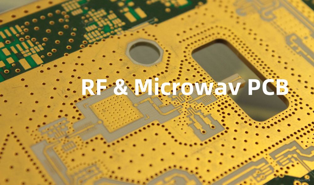
ENIG plating is commonly used for high-frequency PCBs due to its excellent electrical conductivity and flatness. The gold layer provides a low-loss surface for high-speed signals, while the nickel layer ensures a smooth surface for consistent impedance.
Fine-Pitch Components
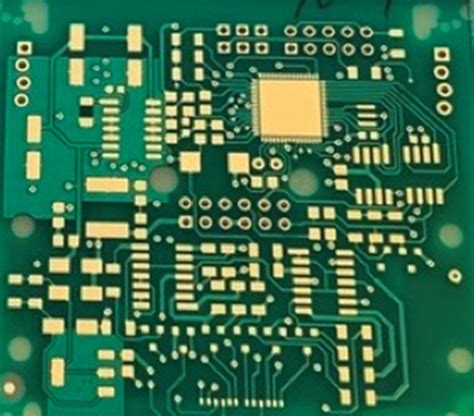
The flatness and solderability of ENIG make it suitable for fine-pitch components, such as Ball Grid Arrays (BGAs) and Quad Flat Packages (QFPs). The gold layer ensures reliable solder joints, while the flat surface prevents tombstoning and other soldering defects.
Wire Bonding
ENIG plating is also used for wire bonding applications, where thin gold or aluminum wires are bonded to the PCB surface. The gold layer provides a compatible surface for thermosonic or ultrasonic bonding, while the nickel layer prevents the formation of brittle intermetallic compounds.

Comparison with Other Surface Finishes
ENIG vs. HASL
Hot Air Solder Leveling (HASL) is another common surface finish that involves dipping the PCB in molten solder and using hot air to level the surface. While HASL is less expensive than ENIG, it has several disadvantages:
| Parameter | ENIG | HASL |
|---|---|---|
| RoHS Compliance | Yes | No (lead-based) |
| Flatness | Excellent | Poor |
| Solderability | Excellent | Good |
| Shelf Life | 12+ months | 6-12 months |
| Cost | High | Low |
ENIG vs. Immersion Silver
Immersion silver is a lead-free surface finish that provides good solderability and conductivity. However, it has some limitations compared to ENIG:
| Parameter | ENIG | Immersion Silver |
|---|---|---|
| Corrosion Resistance | Excellent | Moderate |
| Shelf Life | 12+ months | 6-12 months |
| Wire Bonding | Yes | No |
| Cost | High | Moderate |
Troubleshooting ENIG Plating Issues
Black Pad
Black pad is a defect that occurs when the nickel layer separates from the copper surface, resulting in a black appearance. It is caused by excessive phosphorus content in the nickel layer, which can be prevented by controlling the plating bath chemistry and using a low-phosphorus nickel.
Gold Porosity
Gold porosity occurs when the gold layer has pinholes or voids, exposing the underlying nickel. It can be caused by contamination in the plating bath or improper surface preparation. Maintaining a clean plating environment and using high-purity chemicals can help prevent gold porosity.
Nickel Corrosion
Nickel corrosion can occur if the gold layer is too thin or porous, allowing moisture to reach the nickel. It can be prevented by ensuring a sufficient gold thickness (2-5 microinches) and minimizing porosity.
Frequently Asked Questions (FAQ)
1. Is ENIG plating suitable for lead-free soldering?
Yes, ENIG plating is compatible with lead-free soldering processes. The gold layer provides excellent solderability and wetting, ensuring reliable solder joints with lead-free solders.
2. How long does ENIG plating last?
ENIG plating has a shelf life of 12 months or more, depending on the storage conditions. Proper packaging and storage in a cool, dry environment can help extend the shelf life.
3. Can ENIG be used for Aluminum PCBs?
No, ENIG plating is not suitable for aluminum PCBs. The electroless plating process requires a catalytic surface, which is typically copper. Aluminum PCBs require different surface finishes, such as Nickel-Gold electroplating or immersion silver.
4. How does the cost of ENIG compare to other surface finishes?
ENIG is one of the more expensive surface finishes due to the use of gold. It is typically more expensive than HASL, OSP, and immersion silver, but less expensive than gold electroplating.
5. Can ENIG be reworked?
Yes, ENIG can be reworked using standard soldering techniques. However, excessive rework can degrade the gold layer and expose the underlying nickel, leading to corrosion. It is recommended to minimize rework and use fresh solder for each rework operation.
Conclusion
Electroless gold-nickel plating is a versatile and reliable surface finish for PCBs. Its excellent solderability, corrosion resistance, and RoHS compliance make it a popular choice for a wide range of applications. By understanding the ENIG plating process, its advantages, and potential issues, PCB manufacturers can produce high-quality boards that meet the demands of the electronics industry.

No responses yet