Introduction to PCB Printing
Printed Circuit Board (PCB) printing is a crucial step in the manufacturing process of electronic devices. It involves the creation of conductive pathways on a non-conductive substrate to connect electronic components. Ensuring that PCB printing is done properly is essential for the proper functioning and reliability of the final product. In this article, we will discuss the various aspects of PCB printing and how to ensure that it is done correctly.
What is PCB Printing?
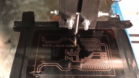
PCB printing is the process of creating conductive pathways on a non-conductive substrate, typically made of fiberglass or plastic, to connect electronic components. The conductive pathways are created using a conductive ink or paste, which is printed onto the substrate using various printing techniques such as screen printing, inkjet printing, or photolithography.
Why is PCB Printing Important?
PCB printing is essential for the proper functioning and reliability of electronic devices. Poorly printed PCBs can lead to a range of issues such as short circuits, open circuits, and signal integrity problems. These issues can cause the device to malfunction or fail entirely, leading to costly repairs or replacements. Properly printed PCBs, on the other hand, ensure that the electronic components are connected correctly and function as intended.
Types of PCB Printing
There are several types of PCB printing techniques, each with its own advantages and disadvantages. The choice of printing technique depends on various factors such as the complexity of the design, the required resolution, and the production volume. Here are some of the most common PCB printing techniques:
Screen Printing
Screen printing is a popular PCB printing technique that involves forcing conductive ink through a mesh screen onto the substrate. The screen is coated with a light-sensitive emulsion that is exposed to light through a film positive of the PCB design. The unexposed areas of the emulsion are then washed away, leaving a stencil of the PCB design on the screen. The conductive ink is then forced through the stencil onto the substrate using a squeegee.
| Advantages | Disadvantages |
|---|---|
| Low cost | Limited resolution |
| High production volume | Requires a separate screen for each design |
| Suitable for simple designs | Not suitable for complex designs |
Inkjet Printing
Inkjet printing is a Digital PCB printing technique that involves depositing conductive ink onto the substrate using a print head. The print head contains a series of nozzles that eject tiny droplets of ink onto the substrate in a precise pattern. The ink is then cured using heat or UV light to create the conductive pathways.
| Advantages | Disadvantages |
|---|---|
| High resolution | High cost |
| Suitable for complex designs | Low production volume |
| Quick turnaround time | Requires specialized equipment |
Photolithography
Photolithography is a high-resolution PCB printing technique that involves exposing a light-sensitive photoresist to light through a photomask of the PCB design. The exposed areas of the photoresist are then developed and etched away, leaving the conductive pathways on the substrate.
| Advantages | Disadvantages |
|---|---|
| High resolution | High cost |
| Suitable for complex designs | Requires specialized equipment |
| High production volume | Lengthy process |

Factors Affecting PCB Printing Quality
Several factors can affect the quality of PCB printing. Here are some of the most important factors to consider:
Substrate Material
The choice of substrate material can affect the quality of PCB printing. Different substrate materials have different surface properties, which can affect the adhesion and resolution of the conductive ink. For example, fiberglass substrates are commonly used for PCBs due to their excellent mechanical and electrical properties, but they can be more difficult to print on compared to plastic substrates.
Ink Formulation
The formulation of the conductive ink can also affect the quality of PCB printing. Different ink formulations have different properties such as viscosity, conductivity, and curing requirements. Choosing the right ink formulation for the specific application and printing technique is crucial for achieving high-quality results.
Printing Parameters
The printing parameters such as the screen mesh count, squeegee pressure, and print speed can also affect the quality of PCB printing. These parameters need to be optimized for the specific substrate material, ink formulation, and printing technique to achieve the desired resolution and conductivity.
Environmental Conditions
Environmental conditions such as temperature and humidity can also affect the quality of PCB printing. High temperature and humidity can cause the ink to dry too quickly or not adhere properly to the substrate, while low temperature and humidity can cause the ink to dry too slowly or not cure properly.

Best Practices for PCB Printing
To ensure that PCB printing is done properly, here are some best practices to follow:
Design for Manufacturability
When designing a PCB, it is important to consider the manufacturability of the design. This includes factors such as the minimum trace width and spacing, the size and shape of the pads, and the placement of components. Designing for manufacturability can help to ensure that the PCB can be printed and assembled correctly.
Choose the Right Printing Technique
Choosing the right printing technique for the specific application and design is crucial for achieving high-quality results. Factors to consider include the complexity of the design, the required resolution, and the production volume.
Optimize Printing Parameters
Optimizing the printing parameters such as the screen mesh count, squeegee pressure, and print speed can help to achieve the desired resolution and conductivity. This may require some trial and error to find the optimal settings for the specific substrate material, ink formulation, and printing technique.
Control Environmental Conditions
Controlling the environmental conditions such as temperature and humidity can help to ensure consistent and high-quality results. This may involve using a climate-controlled printing environment or adjusting the printing parameters to compensate for changes in environmental conditions.
Implement Quality Control Measures
Implementing quality control measures such as visual inspection, electrical testing, and cross-sectioning can help to identify and correct any issues with the printed PCBs. This can help to ensure that the final product meets the required specifications and functions as intended.

Frequently Asked Questions (FAQ)
1. What is the minimum trace width and spacing for PCB printing?
The minimum trace width and spacing for PCB printing depends on the printing technique and the substrate material. For screen printing, the minimum trace width and spacing is typically around 0.2 mm, while for inkjet printing and photolithography, it can be as low as 0.05 mm.
2. Can PCBs be printed on flexible substrates?
Yes, PCBs can be printed on flexible substrates such as polyimide or PET. However, the printing process may need to be modified to accommodate the flexibility of the substrate, and the choice of ink formulation may need to be adjusted to ensure proper adhesion and conductivity.
3. How long does it take to print a PCB?
The time it takes to print a PCB depends on the printing technique and the complexity of the design. Screen printing can typically produce a PCB in a few minutes, while inkjet printing and photolithography may take several hours or even days for complex designs.
4. What is the typical cost of PCB printing?
The cost of PCB printing depends on various factors such as the printing technique, the substrate material, the ink formulation, and the production volume. Screen printing is typically the most cost-effective option for high-volume production, while inkjet printing and photolithography may be more expensive due to the specialized equipment and materials required.
5. Can PCBs be printed with multiple layers?
Yes, PCBs can be printed with multiple layers to increase the circuit density and functionality. This involves printing and aligning multiple layers of conductive pathways and insulating materials. The number of layers that can be printed depends on the printing technique and the substrate material, but it is not uncommon to see PCBs with up to 16 layers or more.
Conclusion
PCB printing is a crucial step in the manufacturing process of electronic devices. Ensuring that PCB printing is done properly is essential for the proper functioning and reliability of the final product. The choice of printing technique, substrate material, ink formulation, and printing parameters can all affect the quality of PCB printing. By following best practices such as designing for manufacturability, choosing the right printing technique, optimizing printing parameters, controlling environmental conditions, and implementing quality control measures, it is possible to achieve high-quality and reliable PCB printing results.
No responses yet