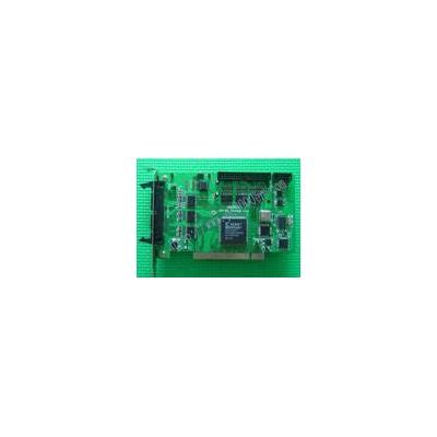
What is PCB Copy?
PCB copy, also known as PCB duplication or PCB cloning, is the process of creating an exact replica of an existing printed circuit board (PCB). This process involves analyzing the original PCB design, identifying its components, and recreating the board with identical functionality. PCB copy is often used when the original design files are unavailable, the original manufacturer is no longer in business, or when reverse engineering is required to understand the functionality of a particular PCB.
Reasons for PCB Copy
There are several reasons why someone might need to create a copy of a PCB:
- Obsolescence: When the original PCB is no longer in production or the manufacturer has discontinued the product.
- Replacement: If a PCB in a critical system fails and needs to be replaced, but the original design files are not available.
- Reverse Engineering: To understand how a particular PCB functions, engineers may need to create a copy and analyze its components and design.
- Cost Reduction: In some cases, creating a PCB copy can be more cost-effective than purchasing the original board from the manufacturer.
The PCB Copy Process
The PCB copy process typically involves several steps, each requiring specific expertise and tools. Below is a table outlining the main stages of PCB copying:
| Step | Description |
|---|---|
| 1. PCB Digitization | The original PCB is scanned or photographed to create a digital image of the board. |
| 2. Image Processing | The digital image is processed to enhance clarity and remove any distortions or artifacts. |
| 3. Layer Separation | If the original PCB is multi-layered, each layer is separated and analyzed individually. |
| 4. Component Identification | The components on the PCB are identified and their specifications are determined. |
| 5. Schematic Creation | Based on the identified components and their connections, a schematic diagram of the PCB is created. |
| 6. PCB Layout | Using the schematic, a new PCB layout is designed, mimicking the original board’s component placement and routing. |
| 7. Fabrication | The new PCB design is sent for fabrication, where it is manufactured according to the specified design. |
| 8. Assembly | The fabricated PCB is then assembled with the identified components, creating a functional replica of the original board. |
| 9. Testing and Verification | The newly created PCB copy is tested and verified to ensure it functions identically to the original board. |
1. PCB Digitization
The first step in the PCB copy process is to create a digital image of the original board. This can be done using various methods, such as:
- High-resolution scanning
- Digital photography
- X-ray imaging (for multi-layered boards)
The goal is to capture a clear, detailed image of the PCB that can be used for further analysis.
2. Image Processing
Once the digital image of the PCB is obtained, it needs to be processed to enhance its clarity and remove any distortions or artifacts. This is typically done using specialized image processing software that can:
- Adjust brightness and contrast
- Remove background noise
- Correct perspective distortions
- Sharpen edges and details
The resulting image should be a clean, high-quality representation of the original PCB.
3. Layer Separation
For multi-layered PCBs, each layer needs to be separated and analyzed individually. This is because the components and traces on each layer may be different and need to be identified separately. Layer separation can be achieved through various methods, such as:
- X-ray imaging
- Micro-Sectioning
- Chemical etching
Once the layers are separated, each one can be analyzed and digitized separately.
4. Component Identification
With the layers separated and the PCB image processed, the next step is to identify the components on the board. This involves:
- Determining the component type (resistor, capacitor, IC, etc.)
- Identifying the component values (resistance, capacitance, part number, etc.)
- Locating the component on the board
Component identification can be done manually by experienced engineers or with the help of automated systems that use computer vision and machine learning algorithms.
5. Schematic Creation
Based on the identified components and their locations on the board, a schematic diagram of the PCB can be created. The schematic shows the electrical connections between components and helps in understanding the overall functionality of the board. Creating a schematic involves:
- Drawing the component symbols
- Connecting the components according to their locations on the board
- Labeling the components with their values and part numbers
- Adding any additional information, such as power supply voltages or signal names
The schematic is an essential part of the PCB copy process, as it serves as the blueprint for the new board design.
6. PCB Layout
With the schematic complete, the next step is to create a new PCB layout that mimics the original board’s component placement and routing. This involves:
- Placing the components on the board according to their locations in the original design
- Routing the traces between the components, following the same path as the original board
- Ensuring that the new layout meets the required design rules and constraints
- Adding any necessary copper pours, vias, or other features
The PCB layout is typically created using specialized PCB design software, such as Altium Designer, Eagle, or KiCad.
7. Fabrication
Once the new PCB layout is complete, it is sent for fabrication. The fabrication process involves:
- Creating a photomask of the PCB layout
- Applying the photomask to a copper-clad board and exposing it to light
- Developing the exposed board to remove the unwanted copper
- Etching the board to create the copper traces and pads
- Drilling any necessary holes for through-hole components
- Applying a solder mask and silkscreen to protect the board and label the components
The fabricated board is then ready for assembly.
8. Assembly
The final step in the PCB copy process is to assemble the board with the identified components. This involves:
- Placing the components on the board according to their locations in the layout
- Soldering the components to the board using either through-hole or surface-mount techniques
- Inspecting the assembled board for any errors or defects
- Cleaning the board to remove any flux residue or contaminants
The assembled board is now a functional replica of the original PCB.
9. Testing and Verification
Before the PCB copy can be considered complete, it needs to be tested and verified to ensure that it functions identically to the original board. This involves:
- Powering up the board and checking for any short circuits or other faults
- Testing the board’s functionality using the same inputs and outputs as the original board
- Comparing the performance of the copy to that of the original board
- Making any necessary adjustments or modifications to the copy to match the original board’s performance
Once the PCB copy has been thoroughly tested and verified, it can be used as a replacement for the original board.

Challenges in PCB Copying
While PCB copying is a valuable process, it is not without its challenges. Some of the main challenges in PCB copying include:
1. Component Obsolescence
One of the biggest challenges in PCB copying is dealing with obsolete components. If the original PCB uses components that are no longer in production, finding suitable replacements can be difficult. In some cases, it may be necessary to redesign the board to use newer, available components.
2. Multi-Layered Boards
Copying multi-layered PCBs can be particularly challenging, as each layer needs to be separated and analyzed individually. This process can be time-consuming and requires specialized equipment and expertise.
3. Intellectual Property Concerns
PCB copying can sometimes raise intellectual property concerns, particularly if the original board design is protected by patents or copyrights. It is important to ensure that any PCB copying is done legally and with the necessary permissions.
4. Quality Control
Ensuring that the PCB copy functions identically to the original board can be a challenge, particularly if the original board’s performance is not well documented. Thorough testing and verification are essential to ensure that the copy meets the required quality standards.

Frequently Asked Questions
1. Is PCB copying legal?
The legality of PCB copying depends on the specific circumstances. If the original PCB design is protected by patents or copyrights, copying it without permission may be illegal. However, if the PCB is being copied for legitimate reasons, such as obsolescence or reverse engineering, and the necessary permissions have been obtained, then PCB copying can be legal.
2. How long does the PCB copy process take?
The time required for PCB copying varies depending on the complexity of the board and the specific methods used. Simple, single-layer boards may be copied in a matter of days, while complex, multi-layered boards can take several weeks or even months to copy.
3. How much does PCB copying cost?
The cost of PCB copying depends on several factors, such as the complexity of the board, the number of layers, and the specific methods used. In general, PCB copying can be more cost-effective than purchasing the original board from the manufacturer, particularly for older or obsolete designs.
4. Can PCB copying be used for any type of board?
In theory, PCB copying can be used for any type of board, regardless of its complexity or application. However, some types of boards, such as those with high-frequency or high-power components, may require specialized copying methods and expertise.
5. What are the benefits of PCB copying?
PCB copying offers several benefits, including:
- Ability to replace obsolete or discontinued boards
- Cost savings compared to purchasing original boards
- Opportunity for reverse engineering and design improvement
- Faster turnaround times compared to custom board design
By leveraging PCB copying, engineers and manufacturers can overcome challenges related to obsolescence, cost, and availability, while ensuring that critical systems remain functional and up-to-date.

Conclusion
PCB copying is a valuable process that allows engineers and manufacturers to create exact replicas of existing printed circuit boards. Whether for obsolescence, replacement, reverse engineering, or cost reduction, PCB copying offers a range of benefits and applications. However, the process is not without its challenges, including component obsolescence, multi-layered board complexity, intellectual property concerns, and quality control. By understanding the PCB copy process, its challenges, and its benefits, engineers and manufacturers can make informed decisions about when and how to use this powerful technique to overcome PCB-related challenges and ensure the continued functionality of critical systems.
No responses yet