What is Back Drill PCB?
Back drill PCB, also known as controlled depth drilling or back-drilling, is a technique used in the manufacturing of printed circuit boards (PCBs) to remove unwanted conductive material from the inner layers of the board. This process is primarily used to eliminate stub resonance and improve signal integrity in high-speed digital designs.
In a multi-layer PCB, vias are used to connect traces on different layers. When a via is drilled through the entire board, it creates a conductive stub that extends beyond the target layer. These stubs can act as tiny antennas, causing signal reflections and degrading the overall signal quality. Back drilling is the process of removing these unwanted stubs to optimize the PCB’s performance.
How Back Drill PCB Works
The back drill process involves using a specialized drill bit to remove the unwanted portion of the via barrel. The drill bit is precisely controlled to stop at a specific depth, ensuring that only the unnecessary part of the via is removed without damaging the target layer or the surrounding traces.
The process typically follows these steps:
- The PCB is first drilled with standard vias that connect all the layers.
- The board is then flipped over, and the back drill process is performed on the appropriate vias.
- The back drill bit is carefully aligned with the center of the via and drilled to the specified depth.
- The unwanted portion of the via barrel is removed, leaving only the necessary connection between the target layers.
Benefits of Back Drill PCB
Back drilling offers several benefits for high-speed Digital PCB designs:
-
Improved Signal Integrity: By removing the unwanted via stubs, back drilling reduces signal reflections and improves the overall signal quality. This is particularly important for high-frequency signals, as the stub effect becomes more pronounced at higher frequencies.
-
Reduced EMI: The removal of via stubs helps to reduce electromagnetic interference (EMI) by minimizing the antenna-like behavior of the stubs. This can be crucial in applications where EMI compliance is a concern.
-
Enhanced Impedance Control: Back drilling allows for better control over the impedance of the vias, as the removal of the stubs reduces the capacitance and inductance associated with the via structure. This can help to maintain consistent impedance throughout the signal path.
-
Increased Bandwidth: By reducing signal distortions and reflections, back drilling can help to increase the usable bandwidth of the PCB. This is essential for high-speed applications that require the transmission of large amounts of data.
When to Use Back Drill PCB
Back drilling is typically used in high-speed digital PCB designs where signal integrity is critical. Some common applications include:
- High-speed communication systems (e.g., 5G, fiber optics)
- High-performance computing (e.g., servers, data centers)
- Aerospace and defense systems
- Medical equipment
- Automotive electronics
In general, back drilling should be considered when the signal frequencies are high enough that the stub effect becomes problematic. This can vary depending on the specific design and the materials used, but a general rule of thumb is to consider back drilling for signals with frequencies above 5 GHz.

Designing for Back Drill PCB
When designing a PCB that will incorporate back drilling, there are several factors to consider:
Via Size and Placement
The size and placement of the vias should be carefully considered to ensure that they can be effectively back drilled. The via diameter should be large enough to allow for the back drill bit to enter and remove the unwanted material without damaging the surrounding traces. Additionally, the vias should be placed in locations that allow for easy access by the back drill machine.
Layer Stack-up
The layer stack-up of the PCB should be designed with back drilling in mind. The target layers for the back drilled vias should be positioned in a way that minimizes the stub length while still maintaining the necessary connections. This may require adjusting the layer stack-up or using blind or buried vias in certain areas.
Drill Depth Control
Accurate control of the back drill depth is crucial to ensure that the unwanted material is removed without damaging the target layer. The design should specify the desired back drill depth for each via, taking into account the thickness of the layers and any tolerances in the manufacturing process.
Signal Routing
When routing signals on a back drilled PCB, it is important to consider the impact of the via stubs on the signal integrity. In some cases, it may be necessary to route signals around the back drilled vias to minimize the stub effect. Additionally, the use of differential pairs and proper trace spacing can help to further improve signal quality.

Implementing Back Drill PCB
Once the PCB has been designed with back drilling in mind, the actual implementation of the process involves several key steps:
Drill File Preparation
The first step in implementing back drilling is to prepare the drill files for the PCB. This involves creating separate drill files for the standard vias and the back drilled vias. The back drill file should specify the location, diameter, and depth of each back drilled via.
Machine Setup
The back drill machine must be properly set up and calibrated to ensure accurate drilling. This involves selecting the appropriate drill bit size and adjusting the machine parameters to match the desired drill depth and speed. The machine should also be equipped with a vision system to ensure precise alignment with the via centers.
Drilling Process
During the drilling process, the PCB is loaded into the back drill machine, and the machine aligns the drill bit with the center of each via specified in the drill file. The machine then drills to the specified depth, removing the unwanted material from the via barrel. This process is repeated for each back drilled via on the board.
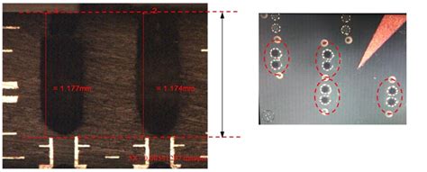
Inspection and Testing
After the back drilling process is complete, the PCB should be thoroughly inspected to ensure that the vias have been properly drilled and that no damage has occurred to the surrounding traces or layers. Electrical testing should also be performed to verify that the board meets the necessary performance specifications.

Challenges and Considerations
While back drilling offers significant benefits for high-speed digital PCBs, there are also several challenges and considerations to keep in mind:
Cost
Back drilling adds an additional step to the PCB manufacturing process, which can increase the overall cost of the board. The cost impact will depend on factors such as the number of back drilled vias, the complexity of the design, and the manufacturing volume.
Manufacturing Complexity
Implementing back drilling requires specialized equipment and expertise, which can increase the complexity of the manufacturing process. This can lead to longer lead times and potential issues with yield and reliability.
Design Constraints
The use of back drilling may impose certain design constraints, such as minimum via sizes and spacing requirements. These constraints must be carefully considered during the design phase to ensure that the board can be effectively manufactured.
Material Selection
The choice of PCB materials can impact the effectiveness of back drilling. Some materials, such as high-frequency laminates, may be more susceptible to damage during the drilling process. The material properties should be carefully considered when designing a back drilled PCB.
Frequently Asked Questions (FAQ)
1. What is the difference between back drilling and controlled depth drilling?
Back drilling and controlled depth drilling are essentially the same process. Both terms refer to the selective removal of unwanted conductive material from the inner layers of a PCB to improve signal integrity. The term “back drilling” is more commonly used in the industry.
2. Can back drilling be used on all types of PCBs?
Back drilling is primarily used on multi-layer PCBs designed for high-speed digital applications. It is not typically necessary or cost-effective for simpler, low-frequency designs. The decision to use back drilling should be based on the specific requirements of the application and the signal frequencies involved.
3. How does back drilling affect the reliability of the PCB?
When properly implemented, back drilling should not have a significant impact on the reliability of the PCB. However, the drilling process does introduce an additional step in the manufacturing process, which can potentially lead to issues if not carefully controlled. Proper machine setup, drill file preparation, and inspection are critical to ensuring the reliability of the finished board.
4. Can back drilling be performed on both through-hole and blind vias?
Yes, back drilling can be performed on both through-hole and blind vias. However, the process may be more challenging for blind vias, as the drill bit must stop at a specific depth within the layer stack-up. Accurate depth control is critical to ensure that the unwanted material is removed without damaging the target layer.
5. Are there any alternatives to back drilling for improving signal integrity?
While back drilling is a highly effective method for improving signal integrity, there are some alternatives that can be considered. These include the use of blind and buried vias, high-frequency laminates, and advanced routing techniques such as differential pairs and serpentine traces. The choice of approach will depend on the specific requirements of the application and the trade-offs between cost, performance, and manufacturability.
Conclusion
Back drill PCB is a powerful technique for improving signal integrity and performance in high-speed digital designs. By selectively removing unwanted conductive material from the inner layers of the board, back drilling can reduce signal reflections, minimize EMI, and increase usable bandwidth.
However, implementing back drilling requires careful consideration of design factors such as via size and placement, layer stack-up, and drill depth control. The manufacturing process also requires specialized equipment and expertise to ensure accurate and reliable results.
When properly implemented, back drilling can provide significant benefits for a wide range of high-speed applications, from communications systems to aerospace and defense. As signal frequencies continue to increase and PCB designs become more complex, the use of back drilling is likely to become increasingly important for maintaining signal integrity and overall system performance.
No responses yet