Introduction
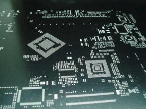
Printed Circuit Board (PCB) stencils are essential tools in the Electronics Manufacturing process. They are used to apply solder paste onto the PCB pads, which is a crucial step in the surface mount technology (SMT) assembly process. Creating precise openings on PCB stencils is critical for ensuring the correct amount of solder paste is deposited on the pads, leading to better soldering quality and fewer defects.
In this article, we will discuss the five best tips for creating openings on PCB Stencils, focusing on achieving the optimal PCB Stencil Openings for your manufacturing needs.
Tip 1: Choose the Right Stencil Thickness
Selecting the appropriate stencil thickness is the first step in creating optimal PCB stencil openings. The stencil thickness directly affects the amount of solder paste deposited on the pads and the ease of solder paste release from the stencil.
Factors Affecting Stencil Thickness Choice
- Component pitch and size
- Solder paste type and viscosity
- PCB pad geometry and surface finish
- Manufacturing process requirements
Common Stencil Thicknesses
| Stencil Thickness (mm) | Typical Applications |
|---|---|
| 0.100 | Fine pitch components (0.3mm – 0.4mm) |
| 0.125 | Standard SMT components (0.5mm – 0.8mm) |
| 0.150 | Larger SMT components (0.8mm – 1.27mm) |
| 0.200 | Power components and connectors |
As a general rule, thinner stencils are better suited for finer pitch components, while thicker stencils are used for larger components and higher volume solder paste deposits.

Tip 2: Optimize Aperture Design
Aperture design refers to the shape, size, and orientation of the openings on the PCB stencil. Optimizing the aperture design is crucial for achieving the desired solder paste deposit volume and shape on the PCB pads.
Aperture Shape
The most common aperture shapes are rectangular and circular. Rectangular apertures are typically used for standard SMT pads, while circular apertures are used for round or oval pads, such as those found on Ball Grid Array (BGA) components.
Aperture Size
Aperture size is determined by the PCB pad size and the desired solder paste volume. A general guideline is to design the aperture size to be slightly larger than the pad size, typically by 10% to 20%. This ensures adequate solder paste coverage on the pad while preventing excessive solder paste deposition.
Aperture Orientation
For rectangular apertures, the orientation should match the orientation of the PCB pads. This ensures proper alignment between the stencil and the PCB during the solder paste printing process.

Tip 3: Consider Area Ratio
Area ratio is the ratio between the aperture opening area and the aperture wall area. It is a critical factor in determining the ease of solder paste release from the stencil apertures.
Calculating Area Ratio
Area Ratio = Aperture Opening Area ÷ Aperture Wall Area
Where:
– Aperture Opening Area = Length × Width (for rectangular apertures)
– Aperture Wall Area = 2 × (Length + Width) × Stencil Thickness
Recommended Area Ratio
For optimal solder paste release, the recommended area ratio is between 0.66 and 0.80. Area ratios below 0.66 may lead to incomplete solder paste release, while ratios above 0.80 may result in excessive solder paste deposition.

Tip 4: Implement Aperture Modifications
Aperture modifications are techniques used to improve solder paste release and prevent solder paste bridging between closely spaced apertures.
Common Aperture Modifications
-
Aperture Tapering: Gradually reducing the aperture size from the top to the bottom of the stencil, creating a trapezoidal shape. This helps in solder paste release and reduces the risk of clogging.
-
Rounded Corners: Adding rounded corners to rectangular apertures to prevent solder paste from accumulating in the corners, which can lead to inconsistent deposits.
-
Aperture Channeling: Creating small channels or slots within the aperture to allow air to escape during solder paste printing, improving paste release.
Aperture Modification Guidelines
| Modification | Guideline |
|---|---|
| Aperture Tapering | Taper angle between 5° and 15° |
| Rounded Corners | Corner radius between 20% and 50% of aperture width |
| Aperture Channeling | Channel width between 10% and 20% of aperture width |
Implementing aperture modifications can significantly improve the solder paste printing process, leading to better soldering quality and reduced defects.
Tip 5: Collaborate with PCB and Stencil Manufacturers
Collaborating with PCB and stencil manufacturers is essential for ensuring the optimal design and fabrication of PCB stencils.
Benefits of Collaboration
-
Expert Advice: PCB and stencil manufacturers have extensive experience in designing and fabricating stencils for various applications. They can provide valuable insights and recommendations based on your specific requirements.
-
Design for Manufacturability (DFM): By collaborating with manufacturers early in the design process, you can ensure that your PCB and stencil designs are optimized for manufacturability, reducing the risk of issues during production.
-
Material Selection: Manufacturers can help you select the best stencil material based on your application, such as stainless steel, nickel, or laser-cut plastic.
-
Prototype and Testing: Working with manufacturers allows you to create prototypes and test your stencil design before mass production, enabling you to identify and address any issues early in the process.
Communication Guidelines
To ensure effective collaboration with PCB and stencil manufacturers, follow these communication guidelines:
-
Provide clear and detailed specifications, including PCB Design files, component information, and manufacturing requirements.
-
Discuss your specific needs and challenges with the manufacturer to benefit from their expertise.
-
Be open to feedback and suggestions from the manufacturer to optimize your stencil design.
-
Maintain open lines of communication throughout the design and manufacturing process to address any issues promptly.
FAQ
1. What is the most common stencil thickness for standard SMT components?
A: The most common stencil thickness for standard SMT components (0.5mm – 0.8mm pitch) is 0.125mm.
2. How much larger should the aperture size be compared to the PCB pad size?
A: As a general guideline, the aperture size should be 10% to 20% larger than the PCB pad size to ensure adequate solder paste coverage while preventing excessive deposition.
3. What is the recommended area ratio for optimal solder paste release?
A: The recommended area ratio for optimal solder paste release is between 0.66 and 0.80.
4. What are the benefits of implementing aperture modifications?
A: Implementing aperture modifications, such as tapering, rounded corners, and channeling, can improve solder paste release, prevent solder paste bridging, and reduce the risk of clogging.
5. Why is collaboration with PCB and stencil manufacturers important?
A: Collaborating with PCB and stencil manufacturers is important for obtaining expert advice, ensuring design for manufacturability, selecting the best materials, and creating prototypes for testing before mass production.
Conclusion
Creating optimal openings on PCB stencils is essential for achieving high-quality solder paste printing and reducing defects in the SMT Assembly process. By following the five tips discussed in this article – choosing the right stencil thickness, optimizing aperture design, considering area ratio, implementing aperture modifications, and collaborating with PCB and stencil manufacturers – you can create PCB stencils that meet your specific manufacturing requirements and ensure the best possible soldering results.
No responses yet