Introduction to LED PCB Manufacturing
Light-emitting diode (LED) technology has revolutionized the lighting industry, offering energy-efficient, long-lasting, and versatile solutions for various applications. The manufacturing and assembly of LED printed circuit boards (PCBs) play a crucial role in the development of high-quality LED products. This article will provide an in-depth overview of the manufacturing and assembly processes for Chip-on-Board (COB) and Surface-Mount Device (SMD) LED PCBs.
Understanding COB and SMD LED Technologies
What are COB LEDs?
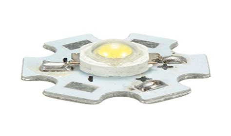
COB LEDs are a type of LED packaging technology where multiple LED chips are directly mounted onto a substrate, such as a PCB or ceramic base. The LED chips are wire-bonded and then encapsulated with a phosphor coating to create a single, uniform light source. COB LEDs offer several advantages, including:
- High luminous efficacy
- Excellent color consistency
- Compact size
- Improved thermal management
What are SMD LEDs?
SMD LEDs are packaged LED components that can be directly soldered onto a PCB using Surface-Mount Technology (SMT). SMD LEDs consist of a single LED chip encased in a small, resin-based package with electrical contacts. They are known for their:
- Small footprint
- Ease of integration
- Wide range of available sizes and colors
- Cost-effectiveness

LED PCB Manufacturing Process
The manufacturing process for LED PCBs involves several critical steps to ensure the production of high-quality, reliable boards.
PCB Design and Layout
- Schematic design: Create a schematic diagram that represents the electrical connections and components of the LED PCB.
- Component placement: Determine the optimal placement of LED components, drivers, and other electronic components on the PCB.
- Routing: Design the copper traces that will connect the components, considering factors such as current capacity, signal integrity, and EMI reduction.
- Design for manufacturability (DFM) checks: Verify that the PCB design adheres to manufacturing guidelines and constraints to ensure smooth production and assembly.
PCB Fabrication
- Material selection: Choose the appropriate PCB substrate material, such as FR-4, aluminum, or ceramic, based on the thermal and mechanical requirements of the LED application.
- Copper clad lamination: Laminate the selected substrate with a layer of copper foil on one or both sides, depending on the PCB design.
- Photoresist application: Apply a light-sensitive photoresist coating to the copper layer(s).
- Exposure and development: Use a photomask to selectively expose the photoresist to UV light, then develop the exposed areas to create the desired circuit pattern.
- Etching: Remove the unwanted copper using a chemical etching process, leaving only the desired circuit traces.
- Soldermask application: Apply a soldermask layer to protect the copper traces and prevent solder bridging during assembly.
- Silkscreen printing: Print component labels, logos, and other markings using a silkscreen process.
- Surface finish: Apply a surface finish, such as HASL, ENIG, or OSP, to protect the exposed copper and improve solderability.
PCB Assembly (PCBA)
- Solder paste application: Apply solder paste to the PCB pads using a stencil or screen printing process.
- SMD component placement: Place SMD LEDs and other components onto the solder paste using a pick-and-place machine or manual assembly methods.
- Reflow soldering: Pass the populated PCB through a reflow oven to melt the solder paste and form permanent electrical and mechanical connections between the components and the PCB.
- COB LED mounting: For COB LED PCBs, mount the COB LED module onto the designated area of the PCB using thermal adhesive or mechanical fasteners.
- Wire bonding: Connect the COB LED module to the PCB using wire bonding techniques, such as gold or aluminum wire bonding.
- Encapsulation: Apply a phosphor coating or encapsulant to protect the COB LED and improve light output and color consistency.
- Inspection and testing: Perform visual inspections, automated optical inspections (AOI), and functional tests to ensure the quality and performance of the assembled LED PCBs.

Key Considerations for LED PCB Manufacturing and Assembly
To ensure the success of LED PCB manufacturing and assembly projects, several key factors must be considered:
Thermal Management
LEDs generate a significant amount of heat during operation, which can negatively impact their performance and lifespan if not properly managed. Effective thermal management strategies include:
- Choosing PCB materials with high thermal conductivity, such as aluminum or Metal-Core PCBs (MCPCBs)
- Incorporating thermal vias and heat sinks to dissipate heat away from the LED components
- Optimizing component placement and PCB layout to minimize thermal hotspots
Optical Design
The optical design of LED PCBs plays a crucial role in determining the light output, distribution, and overall performance of the LED system. Key considerations include:
- Selecting the appropriate LED components based on the desired color temperature, luminous flux, and viewing angle
- Designing reflectors, lenses, and diffusers to shape and control the light output
- Optimizing the spacing and arrangement of LEDs to achieve uniform illumination and minimize color variations
Electrical Design
Proper electrical design ensures that the LED PCB operates safely and efficiently. Important factors to consider include:
- Selecting the appropriate LED driver and power supply based on the voltage and current requirements of the LED components
- Designing the PCB to minimize voltage drop and ensure consistent current distribution across the LED array
- Implementing protection features, such as ESD protection and reverse polarity protection, to safeguard the LED components and circuitry
Quality Control and Testing
Implementing robust quality control measures and thorough testing procedures is essential to ensure the reliability and performance of LED PCBs. Key steps include:
- Performing incoming quality control (IQC) inspections on raw materials and components
- Conducting in-process quality checks during PCB fabrication and assembly
- Performing functional testing, burn-in testing, and environmental testing to validate the performance and durability of the assembled LED PCBs
- Implementing traceability measures, such as barcode scanning and lot tracking, to enable efficient problem-solving and root cause analysis

Advanced LED PCB Manufacturing Techniques
As the LED industry continues to evolve, new manufacturing techniques and technologies are emerging to improve the performance, efficiency, and cost-effectiveness of LED PCBs.
3D Printed Electronics
3D printing technology is being leveraged to create innovative LED PCB designs with complex geometries and embedded electronics. Benefits of 3D printed LED PCBs include:
- Rapid prototyping and iterative design
- Customization and design flexibility
- Integration of multiple components and functionalities into a single, compact package
Flexible and Stretchable LED PCBs
The development of flexible and stretchable LED PCBs opens up new possibilities for wearable electronics, automotive lighting, and other applications that require conformable or bendable light sources. Key enabling technologies include:
- Flexible PCB materials, such as polyimide and thermoplastic polyurethane (TPU)
- Stretchable interconnects and conductive inks
- Thin, flexible LED packages and encapsulation materials
Wafer-Level Packaging (WLP)
Wafer-level packaging is an advanced LED packaging technology that involves packaging individual LED chips at the wafer level before singulation. Benefits of WLP for LED PCBs include:
- Reduced package size and higher packing density
- Improved thermal performance and reliability
- Lower packaging costs and higher throughput
Frequently Asked Questions (FAQ)
- What are the main differences between COB and SMD LEDs?
COB LEDs consist of multiple LED chips mounted directly onto a substrate and encapsulated as a single light source, while SMD LEDs are individual, packaged LED components that can be surface-mounted onto a PCB. COB LEDs offer higher luminous efficacy, better color consistency, and improved thermal management, while SMD LEDs are known for their small size, ease of integration, and cost-effectiveness.
- What factors should I consider when choosing a PCB material for my LED application?
When selecting a PCB material for an LED application, consider factors such as thermal conductivity, thermal expansion, mechanical stability, and cost. FR-4 is a common choice for general-purpose LED PCBs, while aluminum and Metal-Core PCBs (MCPCBs) are preferred for applications that require enhanced thermal management. Ceramic substrates are often used in high-power and high-reliability LED applications.
- How can I ensure good thermal management in my LED PCB design?
To ensure effective thermal management in your LED PCB design, consider the following strategies:
- Choose PCB materials with high thermal conductivity
- Incorporate thermal vias and heat sinks to dissipate heat away from the LED components
- Optimize component placement and PCB layout to minimize thermal hotspots
-
Use thermal interface materials (TIMs) to improve heat transfer between the LED components and the PCB substrate
-
What are some common quality control measures in LED PCB manufacturing?
Common quality control measures in LED PCB manufacturing include:
- Incoming quality control (IQC) inspections on raw materials and components
- In-process quality checks during PCB fabrication and assembly, such as automated optical inspection (AOI) and X-ray inspection
- Functional testing, burn-in testing, and environmental testing to validate the performance and durability of the assembled LED PCBs
-
Implementation of traceability measures, such as barcode scanning and lot tracking, to enable efficient problem-solving and root cause analysis
-
What are the benefits of using 3D printing technology for LED PCB manufacturing?
3D printing technology offers several benefits for LED PCB manufacturing, including:
- Rapid prototyping and iterative design, enabling faster time-to-market and reduced development costs
- Customization and design flexibility, allowing for the creation of complex geometries and embedded electronics
- Integration of multiple components and functionalities into a single, compact package, reducing assembly complexity and improving system reliability
Conclusion
COB and SMD LED PCB manufacturing and assembly involve a complex interplay of design, fabrication, and assembly processes. By understanding the key considerations and best practices in LED PCB manufacturing, designers and engineers can create high-quality, reliable, and efficient LED systems for a wide range of applications. As new technologies and techniques continue to emerge, the LED industry is poised for further innovation and growth, driving the development of ever-more sophisticated and performance-driven LED PCB solutions.
No responses yet