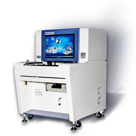
How Does Automated Optical Inspection Work?
AOI systems typically consist of the following components:
- High-resolution cameras
- Lighting system
- Image processing software
- Conveyor system
The PCB is placed on the conveyor system, which moves it through the AOI machine. As the PCB passes under the cameras, images are captured from various angles and lighting conditions. These images are then analyzed by the image processing software, which compares them to a reference image of a defect-free PCB.
The software uses advanced algorithms to detect various types of defects, such as:
- Solder bridges
- Open circuits
- Short circuits
- Missing or misaligned components
- Insufficient or excessive solder
- Incorrect component polarity
If a defect is detected, the AOI system alerts the operator and marks the location of the defect on the PCB. The operator can then remove the defective PCB from the production line for further inspection or rework.
Benefits of Automated Optical Inspection
AOI offers several benefits over manual inspection methods:
-
Increased accuracy: AOI systems can detect defects that are too small to be seen by the human eye, ensuring a higher level of Quality Control.
-
Faster inspection: AOI systems can inspect PCBs much faster than manual methods, allowing for higher production throughput.
-
Reduced labor costs: By automating the inspection process, AOI systems reduce the need for manual labor, resulting in lower labor costs.
-
Improved consistency: AOI systems provide consistent and repeatable inspection results, eliminating the variability associated with manual inspection.
-
Early defect detection: By detecting defects early in the manufacturing process, AOI systems can prevent defective PCBs from reaching later stages of assembly, reducing waste and rework costs.

Types of Automated Optical Inspection Systems
There are two main types of AOI systems used in PCB manufacturing:
-
2D AOI: These systems use cameras to capture two-dimensional images of the PCB surface. They are effective at detecting defects such as solder bridges, open circuits, and missing components.
-
3D AOI: These systems use structured light or laser scanning to create a three-dimensional image of the PCB surface. They can detect defects that are difficult to see in 2D images, such as insufficient or excessive solder, lifted leads, and component height variations.
Some advanced AOI systems combine both 2D and 3D inspection capabilities for a more comprehensive defect detection process.

Implementing Automated Optical Inspection in PCB Manufacturing
To successfully implement AOI in a PCB manufacturing process, consider the following steps:
-
Define inspection requirements: Determine the types of defects that need to be detected and the required level of accuracy.
-
Select an appropriate AOI system: Choose an AOI system that meets the inspection requirements and is compatible with the existing manufacturing process.
-
Develop inspection programs: Create inspection programs that define the reference images, defect criteria, and inspection parameters for each PCB type.
-
Train operators: Provide training to operators on how to use the AOI system and interpret the inspection results.
-
Establish quality control procedures: Develop procedures for handling defective PCBs and implementing corrective actions to prevent recurring defects.
-
Monitor and optimize performance: Regularly monitor the performance of the AOI system and make adjustments as needed to optimize defect detection and minimize false positives.

Limitations of Automated Optical Inspection
While AOI is a powerful tool for detecting PCB defects, it does have some limitations:
-
Limited depth perception: 2D AOI systems may have difficulty detecting defects that are hidden beneath components or have minimal surface area.
-
False positives and false negatives: AOI systems can sometimes identify non-defective areas as defects (false positives) or miss actual defects (false negatives). Careful programming and optimization of inspection parameters can help minimize these occurrences.
-
Inability to detect functional defects: AOI systems can only detect visible defects and cannot identify functional issues that may arise from incorrect component values or faulty circuit design.
Despite these limitations, AOI remains an essential tool for ensuring the quality and reliability of PCBs in modern Electronics Manufacturing.
Automated Optical Inspection vs. Other Inspection Methods
In addition to AOI, there are other inspection methods used in PCB manufacturing, such as:
-
Manual visual inspection: Human operators visually inspect PCBs for defects using magnifying lenses or microscopes. While manual inspection can catch some defects that AOI may miss, it is slower, less consistent, and more prone to human error.
-
In-circuit testing (ICT): ICT involves using a bed-of-nails fixture to make electrical contact with the PCB and test the functionality of individual components and circuits. ICT can detect functional defects that AOI cannot, but it is more time-consuming and requires specialized fixtures for each PCB design.
-
X-ray inspection: X-ray systems use high-energy radiation to create images of the internal structure of the PCB, allowing for the detection of defects such as voids in solder joints or misaligned ball grid array (BGA) components. X-ray inspection is often used in conjunction with AOI to provide a more comprehensive defect detection solution.
The choice of inspection method depends on factors such as the complexity of the PCB design, the required level of quality control, and the available budget and resources.
Future Trends in Automated Optical Inspection
As PCB designs become more complex and miniaturized, AOI technology must continually evolve to keep pace with the changing requirements of the electronics industry. Some of the future trends in AOI include:
-
Increased use of artificial intelligence: AI-powered AOI systems can learn from past inspection data to improve defect detection accuracy and reduce false positives.
-
Integration with other inspection methods: Combining AOI with other inspection technologies, such as X-ray or ICT, can provide a more comprehensive and efficient defect detection solution.
-
Inline AOI: Integrating AOI systems directly into the production line allows for real-time defect detection and correction, reducing the need for separate inspection stages and improving overall manufacturing efficiency.
-
Adaptive lighting: Advanced AOI systems may incorporate adaptive lighting technology that can automatically adjust the lighting conditions to optimize defect detection for different PCB surfaces and components.
As these trends continue to shape the future of AOI, PCB Manufacturers will be better equipped to meet the ever-increasing quality demands of the electronics industry.
Conclusion
Automated Optical Inspection is a crucial quality control process in PCB manufacturing, offering significant benefits over manual inspection methods in terms of accuracy, speed, consistency, and cost-effectiveness. By understanding the capabilities and limitations of AOI and implementing it effectively within the manufacturing process, PCB manufacturers can ensure the highest levels of product quality and reliability.
As PCB technology continues to advance, AOI systems will play an increasingly important role in maintaining the quality and integrity of electronic devices across a wide range of industries, from consumer electronics to aerospace and beyond.
FAQ
-
Q: What is the difference between 2D and 3D AOI systems?
A: 2D AOI systems use cameras to capture two-dimensional images of the PCB surface, while 3D AOI systems use structured light or laser scanning to create a three-dimensional image of the PCB. 3D AOI can detect defects that are difficult to see in 2D images, such as insufficient or excessive solder, lifted leads, and component height variations. -
Q: Can AOI detect all types of PCB defects?
A: While AOI is effective at detecting a wide range of visible defects, such as solder bridges, open circuits, and missing components, it cannot identify functional defects that may arise from incorrect component values or faulty circuit design. AOI is often used in conjunction with other inspection methods, such as in-circuit testing or X-ray inspection, to provide a more comprehensive defect detection solution. -
Q: How does AOI compare to manual visual inspection?
A: AOI offers several advantages over manual visual inspection, including higher accuracy, faster inspection speeds, reduced labor costs, and improved consistency. However, manual inspection can sometimes catch defects that AOI may miss, particularly in cases where human judgment and experience are required. -
Q: What factors should be considered when implementing AOI in a PCB manufacturing process?
A: When implementing AOI, PCB manufacturers should consider factors such as the types of defects that need to be detected, the required level of accuracy, compatibility with existing manufacturing processes, operator training requirements, and quality control procedures for handling defective PCBs and implementing corrective actions. -
Q: What are some of the future trends in AOI technology?
A: Future trends in AOI include increased use of artificial intelligence for improved defect detection accuracy, integration with other inspection methods for more comprehensive defect detection, inline AOI for real-time defect detection and correction, and adaptive lighting technology for optimized defect detection on different PCB surfaces and components.
| Inspection Method | Advantages | Disadvantages |
|---|---|---|
| Automated Optical Inspection (AOI) | High accuracy, fast inspection speeds, reduced labor costs, improved consistency | Limited depth perception, potential for false positives/negatives, inability to detect functional defects |
| Manual Visual Inspection | Can catch defects missed by AOI, human judgment and experience | Slower, less consistent, more prone to human error |
| In-Circuit Testing (ICT) | Can detect functional defects | Time-consuming, requires specialized fixtures for each PCB design |
| X-Ray Inspection | Can detect internal defects, such as voids in solder joints or misaligned BGA components | More expensive, potential for radiation safety concerns |
No responses yet