Introduction to Copper PCB
Printed Circuit Boards (PCBs) are the backbone of modern electronics. They provide a platform for mounting and interconnecting electronic components, enabling the creation of complex circuits and devices. Among the various types of PCBs, copper-based PCBs are the most commonly used due to their excellent electrical conductivity, durability, and cost-effectiveness. In this article, we will delve into the world of Copper PCBs, exploring their properties, manufacturing processes, applications, and more.
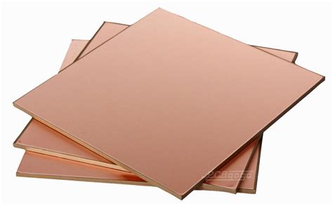
What is a Copper PCB?
A copper PCB is a printed circuit board that uses copper as the primary conductive material for its traces and pads. The copper layer is laminated onto a non-conductive substrate, typically made of materials such as FR-4 (a type of fiberglass-reinforced epoxy resin), polyimide, or ceramic. The copper traces on the PCB act as electrical pathways, allowing signals and power to flow between components mounted on the board.
Advantages of Copper PCBs
Copper PCBs offer several advantages over other types of PCBs:
- Excellent Electrical Conductivity: Copper has a high electrical conductivity, which allows for efficient and reliable signal transmission.
- Thermal Conductivity: Copper is also an excellent thermal conductor, helping to dissipate heat generated by components on the PCB.
- Durability: Copper PCBs are resistant to corrosion and have a long lifespan, making them suitable for various environmental conditions.
- Cost-Effective: Copper is relatively inexpensive compared to other conductive materials, making copper PCBs an economical choice for electronic products.

Manufacturing Process of Copper PCBs
The manufacturing process of copper PCBs involves several steps, each requiring precision and attention to detail. Let’s take a closer look at the key stages:
1. PCB Design and Layout
The first step in creating a copper PCB is designing the circuit and laying out the components on the board. This is typically done using Electronic design Automation (EDA) software, such as Altium Designer, Eagle, or KiCad. The designer creates a schematic diagram of the circuit and then converts it into a physical layout, determining the placement of components and routing of copper traces.
2. Substrate Preparation
Once the PCB design is finalized, the next step is to prepare the substrate. The substrate is typically a laminate material, such as FR-4, which is cut to the desired size and shape. The substrate is then cleaned to remove any contaminants that may affect the adhesion of the copper layer.
3. Copper Lamination
The cleaned substrate is then laminated with a thin layer of copper foil. This is done by applying heat and pressure to bond the copper foil to the substrate. The thickness of the copper layer can vary depending on the specific requirements of the PCB, with common thicknesses ranging from 0.5 oz to 2 oz per square foot.
4. Photoresist Application and Exposure
A photoresist layer is applied to the copper-laminated substrate. The photoresist is a light-sensitive material that hardens when exposed to ultraviolet (UV) light. The PCB layout is then printed onto a transparent film, known as a photomask, which is placed on top of the photoresist-coated copper layer. The board is then exposed to UV light, causing the photoresist to harden in areas not covered by the photomask.
5. Etching
After the exposure process, the PCB is placed in an etching solution, typically containing ferric chloride or ammonium persulfate. The etching solution removes the copper that is not protected by the hardened photoresist, leaving behind the desired copper traces and pads as defined by the PCB layout.
6. Photoresist Removal and Inspection
Once the etching process is complete, the remaining photoresist is removed using a chemical stripper. The PCB is then inspected for any defects or irregularities, such as broken traces or short circuits. If any issues are found, they are corrected before proceeding to the next step.
7. Solder Mask Application
A solder mask layer is applied to the PCB to protect the copper traces and prevent solder bridges during the component assembly process. The solder mask is typically a green or other colored polymer that is applied using a screen printing or photoimaging process. Openings in the solder mask are left for the component pads and any other areas that require soldering.
8. Silkscreen Printing
The final step in the PCB manufacturing process is silkscreen printing. This involves adding text, logos, and other markings to the PCB for identification and assembly purposes. The silkscreen layer is typically white and is applied using a screen printing process.

Types of Copper PCBs
Copper PCBs can be classified based on the number of copper layers and their arrangement. The most common types are:
1. Single-Sided PCBs
Single-sided PCBs have copper traces on only one side of the substrate. They are the simplest and most cost-effective type of PCB, suitable for basic electronic circuits with low component density.
2. Double-Sided PCBs
Double-sided PCBs have copper traces on both sides of the substrate, allowing for a higher component density and more complex circuit designs. The two copper layers are connected using through-hole vias, which are small holes drilled through the board and plated with copper.
3. Multi-Layer PCBs
Multi-layer PCBs consist of three or more copper layers laminated together with insulating material between each layer. They offer the highest component density and are used for complex, high-speed electronic devices. The layers are interconnected using through-hole or blind and buried vias.

Applications of Copper PCBs
Copper PCBs find applications in a wide range of industries and products, including:
- Consumer Electronics: Smartphones, laptops, televisions, and home appliances
- Automotive Industry: Engine control units, infotainment systems, and sensors
- Medical Devices: Diagnostic equipment, patient monitoring systems, and implantable devices
- Industrial Automation: Control systems, sensors, and communication devices
- Aerospace and Defense: Avionics, radar systems, and satellite communication devices
Copper PCB Design Considerations
When designing a copper PCB, several factors must be considered to ensure optimal performance and reliability:
1. Trace Width and Spacing
The width of the copper traces and the spacing between them are critical factors in PCB design. Trace width determines the current-carrying capacity of the trace, while spacing affects signal integrity and electromagnetic compatibility (EMC). The designer must follow the PCB manufacturer’s design rules and guidelines to ensure proper trace width and spacing.
2. Via Size and Placement
Vias are used to interconnect different layers of a multi-layer PCB or to create electrical connections between components on opposite sides of a double-sided PCB. The size and placement of vias must be carefully considered to minimize signal loss and maintain signal integrity.
3. Component Placement
The placement of components on the PCB is crucial for several reasons. It affects signal integrity, thermal management, and the overall size and shape of the PCB. Components should be placed in a way that minimizes the length of copper traces and allows for efficient routing.
4. Grounding and Shielding
Proper grounding and shielding techniques are essential for minimizing electromagnetic interference (EMI) and ensuring signal integrity. The PCB designer must create a robust grounding scheme and use shielding techniques, such as ground planes and shielding cans, to protect sensitive circuits from interference.
PCB Copper Weight and Thickness
The thickness of the copper layer on a PCB is typically specified in terms of copper weight per square foot. The most common copper weights are:
| Copper Weight (oz/ft²) | Nominal Thickness (mm) | Nominal Thickness (mils) |
|---|---|---|
| 0.5 | 0.017 | 0.7 |
| 1 | 0.034 | 1.4 |
| 2 | 0.068 | 2.8 |
| 3 | 0.102 | 4.2 |
| 4 | 0.136 | 5.6 |
The choice of copper weight depends on the current-carrying requirements of the PCB and the desired trace width and spacing. Higher copper weights allow for wider traces and higher current-carrying capacity but may increase the cost and weight of the PCB.
Copper PCB Surface Finishes
After the PCB manufacturing process, a surface finish is applied to the exposed copper areas to protect them from oxidation and enhance solderability. Some common surface finishes for copper PCBs include:
- Hot Air Solder Leveling (HASL): A tin-lead alloy is applied to the copper surfaces using a hot air leveling process. HASL provides excellent solderability but may result in an uneven surface.
- Electroless Nickel Immersion Gold (ENIG): A layer of nickel is deposited on the copper surfaces, followed by a thin layer of gold. ENIG offers a flat surface and good solderability but is more expensive than HASL.
- Organic Solderability Preservative (OSP): A thin, organic coating is applied to the copper surfaces to protect them from oxidation. OSP is cost-effective and provides good solderability but has a limited shelf life.
- Immersion Silver: A thin layer of silver is deposited on the copper surfaces, providing good solderability and a flat surface. Immersion silver is a cost-effective alternative to ENIG.
The choice of surface finish depends on the specific requirements of the PCB, such as the type of components being used, the soldering process, and the environmental conditions the PCB will be exposed to.
Copper PCB Testing and Inspection
To ensure the quality and reliability of copper PCBs, various testing and inspection methods are employed during and after the manufacturing process. Some common techniques include:
- Automated Optical Inspection (AOI): An automated system uses high-resolution cameras to inspect the PCB for defects such as missing components, solder bridges, and incorrect component placement.
- X-Ray Inspection: X-ray imaging is used to inspect the internal structure of the PCB, particularly for multi-layer boards and to detect voids in solder joints.
- In-Circuit Testing (ICT): An automated test system probes the PCB and verifies the functionality of individual components and the interconnections between them.
- Functional Testing: The assembled PCB is powered on and tested for its intended functionality, ensuring that it meets the specified performance requirements.
These testing and inspection methods help identify and correct any issues before the PCB is integrated into the final product, reducing the risk of failures and improving overall reliability.
Frequently Asked Questions (FAQ)
-
What is the difference between a copper PCB and a regular PCB?
A copper PCB specifically refers to a printed circuit board that uses copper as the conductive material for its traces and pads. In contrast, a regular PCB is a more general term that can refer to any type of printed circuit board, regardless of the conductive material used. -
Why is copper used in PCBs?
Copper is used in PCBs due to its excellent electrical conductivity, which allows for efficient and reliable signal transmission. Additionally, copper has good thermal conductivity, helping to dissipate heat generated by components on the PCB. Copper is also relatively inexpensive compared to other conductive materials, making it a cost-effective choice for PCB manufacturing. -
Can copper PCBs be recycled?
Yes, copper PCBs can be recycled. The recycling process typically involves shredding the PCBs and then using various separation techniques, such as density separation and electrostatic separation, to extract the copper and other valuable materials. Recycling copper PCBs helps to conserve natural resources and reduce electronic waste in landfills. -
How do I choose the right copper weight for my PCB?
The choice of copper weight depends on the current-carrying requirements of your PCB and the desired trace width and spacing. Higher copper weights allow for wider traces and higher current-carrying capacity but may increase the cost and weight of the PCB. It’s essential to consult with your PCB manufacturer and follow their design guidelines to select the appropriate copper weight for your specific application. -
What is the typical lifespan of a copper PCB?
The lifespan of a copper PCB depends on various factors, such as the quality of the materials used, the manufacturing process, and the environmental conditions the PCB is exposed to. In general, a well-designed and manufactured copper PCB can last for several years or even decades, depending on the application. Proper handling, storage, and use of the PCB can help extend its lifespan and ensure reliable performance over time.
Conclusion
Copper PCBs are an essential component in modern electronics, offering excellent electrical conductivity, durability, and cost-effectiveness. Understanding the properties, manufacturing processes, and design considerations of copper PCBs is crucial for engineers, designers, and technicians working in the electronics industry.
From single-sided to multi-layer boards, copper PCBs find applications in a wide range of industries, including consumer electronics, automotive, medical devices, industrial automation, and aerospace. Advances in PCB manufacturing technologies and materials continue to push the boundaries of what is possible with copper PCBs, enabling the development of more complex, high-performance electronic devices.
As the demand for electronic products continues to grow, the importance of copper PCBs in the electronics industry is set to increase. By staying up-to-date with the latest trends and best practices in copper PCB design and manufacturing, professionals in the field can create innovative, reliable, and cost-effective electronic solutions that meet the evolving needs of consumers and businesses alike.
No responses yet