What is PCB Prototype Manufacturing?
PCB prototype manufacturing is the process of creating a small batch of printed circuit boards for testing and validation purposes before mass production. This process involves several steps, including design, fabrication, and assembly. The main goal of PCB prototype manufacturing is to ensure that the design is functional, reliable, and meets the required specifications.
PCB Design
The first step in PCB prototype manufacturing is the design phase. This involves creating a schematic diagram and a layout of the PCB using specialized software such as Altium Designer, Eagle, or KiCad. The schematic diagram represents the electrical connections between components, while the layout shows the physical placement of components on the board.
During the design phase, engineers consider various factors such as component selection, signal integrity, power distribution, and thermal management. They also follow design guidelines and industry standards to ensure that the PCB is manufacturable and meets the required specifications.
PCB Fabrication
Once the design is finalized, the next step is PCB fabrication. This process involves converting the digital design files into physical printed circuit boards. The fabrication process typically includes the following steps:
-
Copper Clad Laminate Preparation: The base material for PCBs is a copper-clad laminate, which consists of a layer of copper bonded to an insulating substrate such as FR-4. The laminate is cut to the required size and cleaned to remove any contaminants.
-
Drilling: Holes are drilled into the laminate to accommodate through-hole components and provide electrical connections between layers. The drilling process is performed using high-speed CNC (Computer Numerical Control) machines.
-
Patterning: The desired circuit pattern is transferred onto the copper layer using a photolithographic process. This involves applying a photoresist layer, exposing it to UV light through a photomask, and developing the resist to reveal the desired pattern.
-
Etching: The exposed copper is removed using a chemical etching process, leaving only the desired circuit pattern on the board.
-
Plating: The holes and exposed copper areas are plated with a thin layer of copper to improve conductivity and protect against oxidation.
-
Solder Mask Application: A solder mask layer is applied to the board to protect the copper traces and prevent accidental short circuits during assembly. The solder mask also provides insulation and improves the aesthetic appearance of the board.
-
Silkscreen Printing: Text, logos, and component identifiers are printed onto the board using a silkscreen printing process. This helps in the assembly process and provides a professional finish to the board.
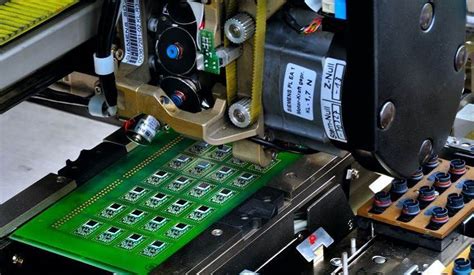
PCB Assembly
After the fabrication process, the PCB is ready for assembly. PCB assembly involves placing and soldering components onto the board. There are two main types of PCB assembly: through-hole and surface mount.
-
Through-Hole Assembly: Through-hole components have long leads that are inserted into the holes drilled in the PCB. The leads are then soldered to the pads on the opposite side of the board. Through-hole assembly is suitable for larger components and provides a strong mechanical connection.
-
Surface Mount Assembly: Surface mount components have small leads or pads that are soldered directly onto the surface of the PCB. Surface mount assembly allows for smaller component sizes and higher component density compared to through-hole assembly.
The PCB assembly process typically involves the following steps:
-
Solder Paste Application: Solder paste, which is a mixture of tiny solder particles and flux, is applied onto the pads using a stencil or syringe. The solder paste holds the components in place during the reflow process.
-
Component Placement: Components are placed onto the PCB using pick-and-place machines or by hand. The placement process requires precise alignment and orientation of the components.
-
Reflow Soldering: The PCB is heated in a reflow oven, causing the solder paste to melt and form a strong electrical and mechanical connection between the components and the pads. The reflow process is carefully controlled to ensure proper solder joint formation and prevent component damage.
-
Inspection and Testing: After the reflow process, the assembled PCB undergoes visual inspection and electrical testing to ensure that all components are properly soldered and functioning as intended. Any defects or issues are identified and corrected at this stage.
Benefits of PCB Prototype Manufacturing
PCB prototype manufacturing offers several benefits in the product development process:
-
Design Validation: PCB prototypes allow designers to validate their designs and ensure that they meet the required specifications before committing to mass production. This helps to identify and fix any design issues early in the development process, saving time and cost.
-
Functionality Testing: Prototypes enable engineers to test the functionality of the PCB and the overall system. This includes verifying the electrical performance, signal integrity, and compatibility with other components.
-
Iterative Improvement: PCB prototypes facilitate iterative design improvements. Based on the feedback and test results from the prototypes, designers can make necessary changes and improvements to optimize the design for performance, reliability, and manufacturability.
-
Cost Savings: Investing in PCB prototypes can lead to significant cost savings in the long run. By identifying and addressing design issues early, manufacturers can avoid costly rework and redesign during mass production. Prototypes also help in optimizing the manufacturing process and reducing production costs.
-
Time-to-Market: PCB prototype manufacturing allows for faster time-to-market by enabling parallel development and testing. While the prototypes are being tested and validated, manufacturers can simultaneously prepare for mass production, reducing the overall development time.

Custom PCB Manufacturer Capabilities
Custom PCB manufacturers offer a range of capabilities to support PCB prototype manufacturing and assembly. These capabilities include:
-
Quick-Turn Prototyping: Custom PCB manufacturers provide fast turnaround times for PCB prototypes, often within a few days. This enables designers to quickly validate their designs and make necessary iterations.
-
Flexible Manufacturing: Custom PCB manufacturers can handle a wide range of PCB designs, including single-sided, double-sided, and multi-layer boards. They also support various materials, surface finishes, and special requirements such as high-frequency or high-temperature applications.
-
Advanced Assembly: Custom PCB manufacturers offer advanced assembly services, including surface mount technology (SMT), through-hole assembly, and mixed assembly. They have the expertise and equipment to handle complex designs and high-density layouts.
-
Quality Control: Custom PCB manufacturers implement strict quality control measures to ensure the reliability and consistency of PCB prototypes. This includes visual inspection, automated optical inspection (AOI), and electrical testing.
-
Design Support: Many custom PCB manufacturers provide design support services to assist customers in optimizing their PCB designs for manufacturability and performance. This includes design rule checks (DRC), design for manufacturing (DFM) analysis, and technical consultation.
-
Inventory Management: Custom PCB manufacturers can help manage inventory for prototype builds, ensuring that components are available when needed and minimizing lead times.

PCB Manufacturing Technologies
Custom PCB manufacturers employ various technologies to produce high-quality PCB prototypes. Some of the key technologies include:
| Technology | Description |
|---|---|
| High-Density Interconnect (HDI) | HDI PCBs feature finer traces, smaller vias, and higher component density, enabling miniaturization and improved performance. |
| Flexible and Rigid-Flex PCBs | Flexible PCBs use flexible substrates to allow bending and folding, while rigid-flex PCBs combine rigid and flexible sections for enhanced design flexibility. |
| Microvia Technology | Microvias are small, laser-drilled vias that provide interconnections between layers in HDI PCBs, enabling higher routing density and improved signal integrity. |
| Embedded Components | Embedded components, such as resistors and capacitors, are placed inside the PCB substrate, reducing board size and improving performance. |
| Controlled Impedance | Controlled impedance PCBs are designed to maintain a specific impedance value for critical signals, minimizing reflections and ensuring signal integrity. |

Challenges in PCB Prototype Manufacturing
While PCB prototype manufacturing offers numerous benefits, it also presents certain challenges that custom PCB manufacturers must address:
-
Design Complexity: As electronic devices become more sophisticated, PCB designs are becoming increasingly complex. Custom PCB manufacturers must have the expertise and tools to handle high-density layouts, fine-pitch components, and advanced packaging technologies.
-
Component Availability: Prototype builds often require specialized or hard-to-find components. Custom PCB manufacturers need to have strong supply chain relationships and inventory management practices to ensure timely availability of components.
-
Time Constraints: PCB prototypes are often required on short notice to meet tight development schedules. Custom PCB manufacturers must have efficient processes and quick-turn capabilities to deliver prototypes within the required timeframe.
-
Cost Considerations: Prototype builds are typically low-volume and may require specialized materials or processes, which can increase costs. Custom PCB manufacturers need to balance cost-effectiveness with the need for high-quality prototypes.
-
Manufacturing Yield: PCB prototypes may have lower manufacturing yields compared to mass production due to the use of new designs, materials, or processes. Custom PCB manufacturers must implement effective quality control measures to minimize defects and ensure consistent prototype quality.
Choosing a Custom PCB Manufacturer
When selecting a custom PCB manufacturer for prototype manufacturing and assembly, consider the following factors:
-
Technical Capabilities: Ensure that the manufacturer has the technical capabilities to handle your specific PCB design requirements, including layer count, material selection, surface finish, and assembly technologies.
-
Experience and Expertise: Look for a manufacturer with extensive experience in PCB prototype manufacturing and a track record of successfully delivering complex projects. Their expertise can provide valuable insights and recommendations for optimizing your design.
-
Quality Standards: Choose a manufacturer that adheres to strict quality standards and has a robust quality management system in place. They should have certifications such as ISO 9001 and IPC standards to ensure consistent quality and reliability.
-
Turnaround Time: Consider the manufacturer’s turnaround time for prototype builds. Quick-turn capabilities are essential for meeting tight development schedules and enabling faster iterations.
-
Customer Support: Evaluate the level of customer support provided by the manufacturer. They should be responsive, communicative, and willing to provide technical assistance throughout the prototyping process.
-
Cost and Value: While cost is an important factor, it should not be the sole determining factor. Consider the overall value provided by the manufacturer, including quality, reliability, technical support, and on-time delivery.
Conclusion
PCB prototype manufacturing and assembly is a critical step in the development of electronic devices. Custom PCB manufacturers play a vital role in bringing ideas to life by providing high-quality PCB prototypes and assembly services. They offer a range of capabilities, including quick-turn prototyping, flexible manufacturing, advanced assembly, quality control, and design support.
When choosing a custom PCB manufacturer, consider their technical capabilities, experience, quality standards, turnaround time, customer support, and overall value. By partnering with a reputable and experienced custom PCB manufacturer, you can ensure the success of your PCB prototype manufacturing and assembly process, leading to faster time-to-market and high-quality electronic products.
FAQ
-
Q: What is the difference between PCB prototype manufacturing and mass production?
A: PCB prototype manufacturing involves creating a small batch of PCBs for testing and validation purposes, while mass production involves producing large quantities of PCBs for commercial use. Prototype manufacturing focuses on design validation, functionality testing, and iterative improvements, while mass production focuses on efficiency, cost-effectiveness, and consistent quality. -
Q: How long does it typically take to manufacture PCB prototypes?
A: The turnaround time for PCB prototype manufacturing varies depending on the complexity of the design and the capabilities of the custom PCB manufacturer. Many manufacturers offer quick-turn prototyping services, with turnaround times ranging from a few days to a couple of weeks. -
Q: What are the advantages of using a custom PCB manufacturer for prototype manufacturing?
A: Custom PCB manufacturers offer several advantages for prototype manufacturing, including technical expertise, flexible manufacturing capabilities, advanced assembly services, strict quality control, and design support. They can handle complex designs, provide quick-turn prototyping, and offer valuable insights for design optimization. -
Q: What should I consider when choosing a custom PCB manufacturer for prototype manufacturing?
A: When choosing a custom PCB manufacturer for prototype manufacturing, consider factors such as their technical capabilities, experience and expertise, quality standards, turnaround time, customer support, and overall value. Look for a manufacturer that can meet your specific design requirements and provide reliable and high-quality prototype services. -
Q: How can PCB prototype manufacturing help in reducing overall development costs?
A: PCB prototype manufacturing can help reduce overall development costs by allowing designers to validate their designs and identify any issues early in the development process. This helps avoid costly rework and redesign during mass production. Prototypes also enable optimization of the manufacturing process, leading to reduced production costs in the long run.
No responses yet