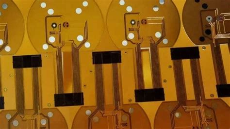
Introduction to Flexible PCBs
Flexible printed circuit boards (PCBs), also known as flex circuits, are a game-changing technology in the world of electronics. Unlike traditional rigid PCBs, flexible PCBs are designed to bend, fold, and twist without losing their electrical functionality. This unique property makes them ideal for applications where space is limited, or where the device needs to conform to a specific shape.
Flexible PCBs are used in a wide range of industries, including:
- Consumer electronics (smartphones, wearables, laptops)
- Medical devices (implantable devices, diagnostic equipment)
- Aerospace and defense (satellites, aircraft, military gear)
- Automotive (dashboard displays, sensors, control modules)
The demand for flexible PCBs has been growing rapidly in recent years, driven by the increasing miniaturization of electronic devices and the need for more reliable and durable solutions.
Advantages of Flexible PCBs
Flexible PCBs offer several advantages over traditional rigid PCBs:
-
Space savings: Flexible PCBs can be bent, folded, and twisted to fit into tight spaces, allowing for more compact and lightweight designs.
-
Improved reliability: The flexible nature of the PCB reduces stress on the components and solder joints, leading to improved reliability and longer product life.
-
Enhanced signal integrity: Flexible PCBs can be designed with controlled impedance and shorter signal paths, resulting in better signal integrity and reduced electromagnetic interference (EMI).
-
Increased design flexibility: Flexible PCBs allow for more creative and innovative product designs, as they can conform to complex shapes and contours.
-
Reduced assembly costs: Flexible PCBs can integrate multiple rigid PCBs into a single flexible assembly, reducing the number of connectors and simplifying the assembly process.

Types of Flexible PCBs
There are three main types of flexible PCBs:
1. Single-sided Flexible PCBs
Single-sided flexible PCBs have conductive traces on only one side of the flexible substrate. They are the simplest and most cost-effective type of flexible PCB, suitable for low-density designs with fewer interconnects.
2. Double-sided Flexible PCBs
Double-sided flexible PCBs have conductive traces on both sides of the flexible substrate, with through-hole vias connecting the top and bottom layers. They offer higher circuit density and more design flexibility compared to single-sided flex PCBs.
3. Multi-layer Flexible PCBs
Multi-layer flexible PCBs consist of three or more conductive layers, separated by flexible insulating layers. They provide the highest circuit density and complexity, allowing for more sophisticated designs and applications.

Flexible PCB Materials
The choice of materials is crucial in the design and manufacturing of flexible PCBs. The most common materials used in flexible PCBs are:
1. Flexible Substrate
-
Polyimide (PI): Polyimide is the most widely used substrate material for flexible PCBs due to its excellent thermal stability, chemical resistance, and mechanical properties. Common brand names include Kapton (DuPont) and Apical (Kaneka).
-
Polyester (PET): Polyester is a lower-cost alternative to polyimide, suitable for less demanding applications. It has good flexibility and electrical properties but lower temperature resistance compared to polyimide.
2. Conductive Layer
- Copper: Copper is the most common conductive material used in flexible PCBs. It is typically available in thicknesses ranging from 9 to 70 microns (µm), with 18 µm and 35 µm being the most popular choices.
3. Adhesive
-
Acrylic: Acrylic adhesives are used to bond the copper foil to the flexible substrate. They offer good adhesion strength, flexibility, and electrical properties.
-
Epoxy: Epoxy adhesives provide higher temperature resistance and better chemical stability compared to acrylic adhesives, but they are less flexible.
4. Coverlay
-
Polyimide: Polyimide coverlays are used to protect the exposed conductive traces and provide electrical insulation. They are available in various thicknesses and can be screen printed or photoimaged.
-
Solder Mask: Solder masks are used to protect the exposed copper traces from oxidation and prevent solder bridging during the assembly process. They are typically applied using screen printing or photoimaging techniques.

Flexible PCB Manufacturing Process
The manufacturing process for flexible PCBs involves several key steps:
1. Design and Artwork Creation
The first step in the flexible PCB manufacturing process is to create the circuit design using PCB design software. The artwork, which includes the conductive traces, vias, and component footprints, is then generated based on the design.
2. Material Selection and Preparation
The appropriate flexible substrate, copper foil, adhesive, and coverlay materials are selected based on the specific requirements of the application. The materials are then cut to size and cleaned to remove any contaminants.
3. Lamination
The flexible substrate, copper foil, and adhesive are laminated together using heat and pressure. This process bonds the layers together and creates a uniform, flexible base material.
4. Drilling and Via Formation
Holes are drilled through the laminated material to create vias that connect the different conductive layers. The holes are then plated with copper to ensure electrical continuity.
5. Patterning and Etching
The desired circuit pattern is transferred onto the copper layer using photolithography. A photoresist is applied to the copper surface, exposed to UV light through a photomask, and developed to create the circuit pattern. The exposed copper is then etched away using a chemical solution, leaving only the desired conductive traces.
6. Coverlay Application
The coverlay material is applied to the etched circuit pattern to provide electrical insulation and protection. The coverlay can be laminated using heat and pressure or applied using adhesive.
7. Surface Finishing
The exposed copper traces are coated with a surface finish to prevent oxidation and improve solderability. Common surface finishes include:
-
HASL (Hot Air Solder Leveling): A tin-lead alloy is applied to the copper traces using a hot air knife, creating a smooth, solderable surface.
-
ENIG (Electroless Nickel Immersion Gold): A thin layer of nickel is deposited onto the copper traces, followed by a layer of gold. ENIG provides excellent solderability and shelf life.
-
OSP (Organic Solderability Preservative): An organic compound is applied to the copper traces, forming a protective layer that prevents oxidation and ensures good solderability.
8. Cutting and Singulation
The finished flexible PCB panel is cut into individual circuits using a variety of methods, such as die-cutting, laser cutting, or routing. The circuits are then inspected for quality and packaged for shipment.
Design Considerations for Flexible PCBs
Designing flexible PCBs requires careful consideration of several factors to ensure optimal performance and reliability:
-
Bend Radius: The minimum bend radius of a flexible PCB depends on the thickness and material properties of the substrate, copper, and coverlay. It is essential to design the circuit with the appropriate bend radius to avoid damaging the traces or components.
-
Stiffener Placement: Stiffeners are used to provide support and stability to certain areas of the flexible PCB, such as connector locations or component mounting areas. Proper placement of stiffeners is crucial to ensure the reliability of the circuit.
-
Trace Width and Spacing: The width and spacing of the conductive traces should be designed to minimize stress during bending and to ensure adequate current carrying capacity. Wider traces and larger spacing can improve flexibility and reliability.
-
Component Selection: Components used on flexible PCBs should be chosen based on their ability to withstand the mechanical stresses associated with bending and flexing. Surface mount components are generally preferred over through-hole components for their lower profile and better mechanical stability.
-
Strain Relief: Incorporating strain relief features, such as curved traces or accordion-style bends, can help distribute stress evenly across the flexible PCB and minimize the risk of trace damage or component failure.
Applications of Flexible PCBs
Flexible PCBs are used in a wide range of applications across various industries. Some notable examples include:
1. Consumer Electronics
-
Smartphones: Flexible PCBs are used in smartphone displays, cameras, and sensors to enable slim, compact designs and improved durability.
-
Wearables: Flexible PCBs are essential in wearable devices, such as smartwatches and fitness trackers, where they conform to the shape of the user’s body and provide reliable performance during movement.
2. Medical Devices
-
Implantable Devices: Flexible PCBs are used in implantable medical devices, such as pacemakers and neurostimulators, where they provide a compact, reliable, and biocompatible solution.
-
Diagnostic Equipment: Flexible PCBs are used in medical diagnostic equipment, such as ultrasound probes and endoscopes, where they enable high-density interconnects and complex shapes.
3. Aerospace and Defense
-
Satellites: Flexible PCBs are used in satellite systems, where they provide lightweight, compact, and reliable solutions for power distribution, signal routing, and thermal management.
-
Military Gear: Flexible PCBs are used in military equipment, such as helmets, vests, and portable communication devices, where they offer ruggedness, flexibility, and high performance in harsh environments.
4. Automotive
-
Dashboard Displays: Flexible PCBs are used in automotive dashboard displays, where they enable slim, curved designs and reliable performance in high-temperature environments.
-
Sensors and Control Modules: Flexible PCBs are used in various automotive sensors and control modules, such as tire pressure monitoring systems and engine control units, where they provide compact, reliable solutions for data acquisition and signal processing.
Frequently Asked Questions (FAQ)
1. What is the difference between flexible and Rigid-Flex PCBs?
Flexible PCBs are entirely flexible, consisting of a flexible substrate, conductive layers, and protective coverlays. Rigid-flex PCBs, on the other hand, are a combination of rigid and flexible sections, where the flexible portions connect the rigid boards. Rigid-flex PCBs offer the benefits of both rigid and flexible PCBs, providing a more structured and stable solution for certain applications.
2. Can flexible PCBs be repaired?
Repairing flexible PCBs can be challenging due to their delicate nature and the specialized materials used in their construction. In most cases, it is more cost-effective and reliable to replace a damaged flexible PCB rather than attempting to repair it. However, minor repairs, such as replacing a damaged component or repairing a broken trace, may be possible depending on the extent of the damage and the skill of the technician.
3. How do you choose the right material for a flexible PCB?
The choice of material for a flexible PCB depends on several factors, including the application requirements, operating environment, and budget. Polyimide is the most common substrate material for high-performance applications due to its excellent thermal stability, chemical resistance, and mechanical properties. For less demanding applications, polyester (PET) can be a lower-cost alternative. The choice of copper thickness, adhesive, and coverlay materials should also be based on the specific requirements of the application, such as bend radius, electrical performance, and environmental resistance.
4. What are the challenges in assembling flexible PCBs?
Assembling flexible PCBs can present several challenges compared to rigid PCBs. Some of the main challenges include:
-
Handling: Flexible PCBs are more delicate and prone to damage during handling and assembly, requiring specialized fixturing and handling techniques.
-
Soldering: The flexible nature of the PCB can make soldering components more difficult, as the board may move or distort during the soldering process. Specialized soldering techniques, such as hot bar soldering or laser soldering, may be required.
-
Component placement: Placing components on a flexible PCB requires precise alignment and control to ensure the components remain stable during the assembly process and in the final application.
-
Strain relief: Proper strain relief techniques must be employed to minimize stress on the components and traces during flexing, ensuring reliable performance over the life of the product.
5. How do you test and inspect flexible PCBs?
Testing and inspecting flexible PCBs involves several techniques to ensure the quality and reliability of the final product. Some common methods include:
-
Visual inspection: A visual examination of the PCB is performed to check for any obvious defects, such as misaligned components, damaged traces, or contamination.
-
Continuity testing: Electrical continuity tests are conducted to verify that all the connections between components and traces are intact and meet the specified resistance requirements.
-
Insulation resistance testing: Insulation resistance tests are performed to ensure that there are no short circuits or leakage paths between adjacent traces or layers.
-
Functional testing: The assembLED PCB is subjected to functional tests to verify that it performs as intended under various operating conditions, such as temperature, humidity, and vibration.
-
Microsectioning: In some cases, microsectioning may be performed to examine the internal structure of the PCB, such as the quality of the plated through-holes, the adhesion between layers, and the integrity of the copper traces.
By employing a combination of these testing and inspection techniques, manufacturers can ensure that the flexible PCBs meet the required quality and reliability standards for their intended applications.
| Characteristic | Rigid PCBs | Flexible PCBs |
|---|---|---|
| Flexibility | Rigid, no bending or flexing | Flexible, can bend and conform to shapes |
| Thickness | Thicker, typically 0.8-3.2 mm | Thinner, typically 0.1-0.3 mm |
| Weight | Heavier | Lighter |
| Durability | Less durable, prone to cracking under stress | More durable, can withstand repeated flexing |
| Design Flexibility | Limited, constrained by rigid shape | High, can conform to complex shapes and contours |
| Cost | Lower cost for simple designs | Higher cost, especially for complex designs |
| Assembly | Easier to assemble, standard processes | More challenging, requires specialized techniques |
| Applications | Consumer electronics, industrial control, telecommunications | Wearables, medical devices, aerospace, automotive |
In conclusion, flexible PCBs offer a unique set of advantages over traditional rigid PCBs, enabling more compact, lightweight, and durable designs for a wide range of applications. By understanding the materials, manufacturing processes, design considerations, and testing techniques involved in flexible PCB production, engineers and designers can create innovative and reliable products that meet the ever-growing demands of the electronics industry.
As technology continues to advance, the use of flexible PCBs is expected to increase across various sectors, from consumer electronics to medical devices, aerospace, and beyond. By staying up-to-date with the latest developments in flexible PCB manufacturing and design, companies can stay ahead of the curve and deliver cutting-edge products that meet the needs of their customers.
No responses yet