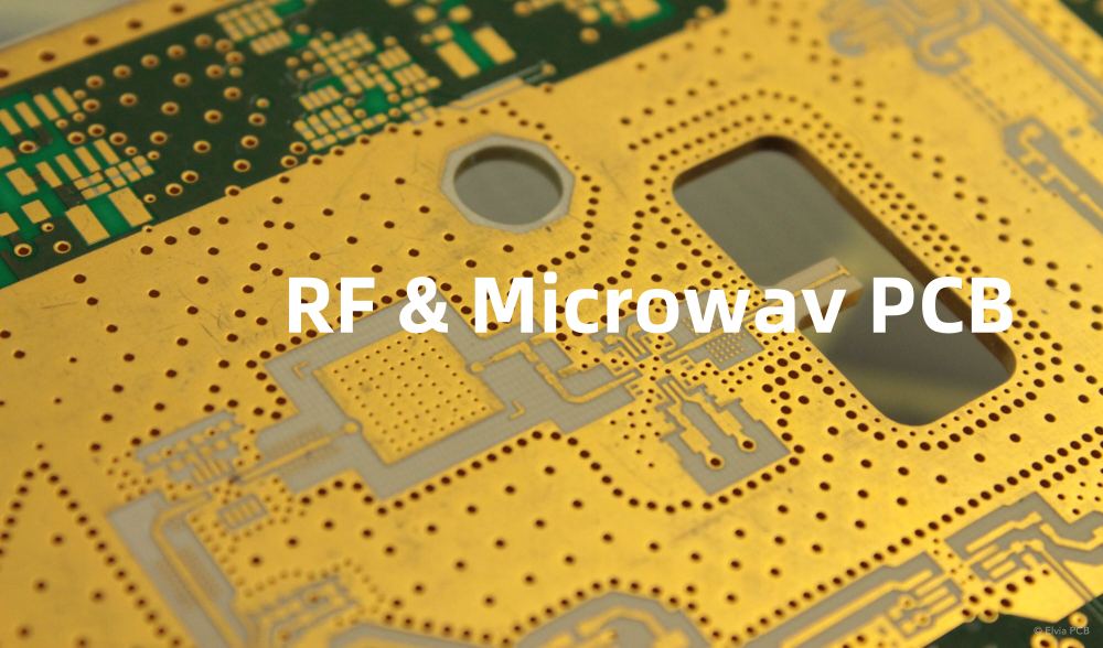
Introduction to Electrostatic Copper Spraying
Electrostatic copper spraying is an advanced technology used in the manufacturing of printed circuit boards (PCBs) with thick copper layers. This innovative process has gained significant attention in the electronics industry due to its ability to produce high-quality, reliable, and cost-effective PCBs. Electrostatic spraying technology allows for the precise and uniform deposition of copper onto the PCB substrate, resulting in superior electrical and thermal properties.
Advantages of Electrostatic Copper Spraying
- Uniform copper distribution
- Increased copper thickness
- Improved electrical conductivity
- Enhanced thermal management
- Cost-effective manufacturing process
The Electrostatic Copper Spraying Process
The electrostatic copper spraying process involves the following key steps:
- Substrate preparation
- Electrostatic charging of copper particles
- Spraying of charged copper particles onto the substrate
- Curing and sintering of the deposited copper layer
Substrate Preparation
Before the electrostatic copper spraying process begins, the PCB substrate must be properly prepared. This includes cleaning the surface to remove any contaminants and applying a conductive seed layer, typically using electroless copper plating. The seed layer provides a conductive surface for the electrostatic spraying process and ensures proper adhesion of the copper layer.
Electrostatic Charging of Copper Particles
In the electrostatic copper spraying process, copper particles are charged using a high-voltage electrostatic field. The charging process is typically performed using a corona discharge or triboelectric charging method. The charged copper particles are then transported to the spraying nozzle using a carrier gas, such as nitrogen or compressed air.
Spraying of Charged Copper Particles onto the Substrate
The charged copper particles are sprayed onto the prepared PCB substrate using a specialized nozzle. The electrostatic attraction between the charged particles and the grounded substrate ensures that the copper particles adhere uniformly to the surface. The spraying process is carefully controlled to achieve the desired thickness and uniformity of the copper layer.
| Parameter | Typical Value |
|---|---|
| Copper particle size | 5-20 μm |
| Electrostatic voltage | 30-100 kV |
| Spraying distance | 10-30 cm |
| Carrier gas pressure | 1-5 bar |
Curing and Sintering of the Deposited Copper Layer
After the electrostatic spraying process, the deposited copper layer undergoes a curing and sintering process to improve its electrical and mechanical properties. The curing process typically involves heating the PCB to a temperature of 150-200°C for a specific duration. During this process, the copper particles fuse together, forming a cohesive and conductive layer.
Benefits of Thick-Copper PCBs Produced by Electrostatic Spraying
Thick-copper PCBs produced using electrostatic spraying technology offer several benefits compared to conventional PCB Manufacturing methods:
- Increased current-carrying capacity
- Improved heat dissipation
- Enhanced mechanical stability
- Reduced signal loss and distortion
- Longer product lifespan
Applications of Thick-Copper PCBs
Thick-copper PCBs are widely used in various industries and applications, including:
- Power electronics
- Automotive electronics
- Renewable energy systems
- High-frequency communication devices
- LED lighting and displays

Challenges and Future Developments
Despite the numerous advantages of electrostatic copper spraying technology, there are still some challenges that need to be addressed:
- Optimization of process parameters for different PCB designs
- Improvement of copper particle size distribution and morphology
- Development of advanced curing and sintering techniques
- Integration with other PCB manufacturing processes
Researchers and industry experts are continuously working on improving electrostatic copper spraying technology to overcome these challenges and further enhance the performance of thick-copper PCBs.
Frequently Asked Questions (FAQ)
-
Q: What is the typical thickness of copper layers achieved using electrostatic spraying?
A: Electrostatic copper spraying can produce copper layers with thicknesses ranging from 50 μm to 500 μm or more, depending on the specific application and process parameters. -
Q: Can electrostatic copper spraying be used for Multilayer PCBs?
A: Yes, electrostatic copper spraying can be used for both single-layer and multilayer PCBs. The process can be repeated to build up multiple thick copper layers with insulating layers in between. -
Q: Is electrostatic copper spraying compatible with other PCB Surface Finishes?
A: Yes, electrostatic copper spraying can be combined with various surface finishes, such as ENIG (Electroless Nickel Immersion Gold), OSP (Organic Solderability Preservative), and HASL (Hot Air Solder Leveling), to provide additional protection and improved solderability. -
Q: How does electrostatic copper spraying compare to other thick-copper PCB manufacturing methods?
A: Electrostatic copper spraying offers several advantages over other methods, such as electroplating or direct bonding copper (DBC). It provides more uniform copper distribution, improved adhesion, and better control over the copper layer thickness. Additionally, it is a more cost-effective and environmentally friendly process. -
Q: What are the environmental considerations associated with electrostatic copper spraying?
A: Electrostatic copper spraying is considered an environmentally friendly process compared to traditional PCB manufacturing methods. It reduces the use of hazardous chemicals and generates less waste. However, proper handling and disposal of copper particles and any byproducts should be ensured to minimize environmental impact.
Conclusion
Electrostatic copper spraying technology has revolutionized the manufacturing of thick-copper PCBs, offering numerous benefits such as uniform copper distribution, improved electrical and thermal properties, and cost-effective production. As the demand for high-performance electronics continues to grow, electrostatic spraying is expected to play an increasingly important role in the PCB industry. With ongoing research and development efforts, this technology will continue to evolve and address the challenges associated with thick-copper PCB manufacturing, ultimately enabling the production of more advanced and reliable electronic devices.

No responses yet