Understanding PCB Repair
Before we dive into the tips, let’s first understand what PCB repair entails. PCB repair is the process of identifying and fixing problems in a PCB to restore its functionality. PCB repair can be necessary due to various reasons, such as:
- Physical damage (e.g., cracks, breaks)
- Component failure
- Corrosion or oxidation
- Manufacturing defects
- Overheating or electrical surges
PCB repair can be a complex process, requiring specialized tools, knowledge, and skills. However, with the right approach and techniques, many PCB issues can be resolved effectively.
Tip 1: Identify the Problem
The first step in PCB repair is to identify the problem accurately. This involves a systematic approach to troubleshooting and diagnosis. Here are some steps to follow:
Visual Inspection
Start by visually inspecting the PCB for any obvious signs of damage, such as:
- Cracks or breaks in the board
- Burnt or discolored components
- Loose or missing components
- Corrosion or oxidation
Use a magnifying glass or microscope to examine the PCB closely, paying attention to the solder joints, traces, and components.
Continuity Testing
Use a multimeter to test for continuity between various points on the PCB. This can help identify any broken traces or short circuits. Check the continuity between:
- Power and ground points
- Input and output pins of components
- Adjacent traces or pads
Functional Testing
If the PCB is part of a larger system, test the functionality of the system as a whole. This can help narrow down the problem to a specific component or section of the PCB.
Schematics and Documentation
Refer to the PCB schematics, layout diagrams, and documentation to understand the intended functionality and connections of the components. This can help identify any discrepancies or anomalies in the actual PCB.
 EMT8u30Ner+GdO0vTLSSDT8iN5VaVzJvd3xjczdK4+W3hJUNFHlSOCgwSO/NdZ4XRI4btG248yPCqMYwMDgcU6WL9vUSa/HQ8rHZSsJTdSMrr01OgQKks5CnawXB9T3rkfHFozaS84HzRSeYfYZrtRu4+UAY6d6ydag+02F5EwB3RuMHoeK7JR9laXr+J49P35cvc838OmOa31G3PPmRCTn6YrlLiPybtlwRtl4Hphq6HwxIY74xt3EkDD0IOKztdt/J1GUY/j3cehNd61gzj+GpY9J8JWkEf2q+iP/AB/RQtKv92VMq2PY8Guuri/A8pktbtCeI3jC+2VzXZiuWjG0Hfubyd3oY+toWs7xR1MEn4/Ka+erxPIu5QuQpbcn0bkV9H6kgaNx/eRh+Yr541eMrcXKHO6CeWM59AxIrOjpUnE6amtKLOh8O3JnlitXlZYpx5b9Pu496oeK9MFtK0kTySLbv5Eu8coCNy5PpWfpNy8MsLhsFHUj1PNdpra6XfW9xItwBLcW6qwx8u9BuUk+vauCrOeHxMZK/K+y/rodVGMa1Fxe/wDX6nmANSdqjYbWI9Dg/WnrXvnj7Di2VKntUB4NTHI5qJ8ZH60IY00ZooqiT6uccsO3BqFxgY7etL5ySHJ4B6fUVXuZY0H7xwqY/HFSQRSOowGYAA8knGT2FZd1cBxKqkpGrcv3cjstJeXMchUyDCqd0cY/ix0LVmXE7zMCeODgL0A9KzlKxx4jGRpLljuJNOXwi8AE/jnuarYx168+9KQTkgc9KQHOQR83pWB89UnKcuaT1CRywHQYAx6mmMxO0EDKr2HJ+tO25yepHY8UzOc5GCO9FiG2BGclmIPv/ShR78FcYPIp25mICqGLHG0jOc8cUs0E8J8uVGSQEZVxggHnNGxdnbmKF1ZJccqAJQcAjuPeqbfuJGhO4MjDr0IIrY+deg5FVri3Ew5/1gyc+9aQnbR7HPVp3Tcdxbe4YJswoB4Jxkmuh0SzkuCZo2H7txx3x7VyS7oBiQ4IbGPb1BruvCrD7PMx/ixtIOeK15dbo0y2HtKyjPoR62J7e6truGHfIi4fjqv40kt9pdzbRSCPyZzneV+U5x6VtazGJLN2wcqM5T72O+K4aBruS4it8F4VkIjdlwwVuoauDEUU013PtKVRU7IdcW6SvIOoYbg3fPrVOAGNuAD1BzW7qKw2oAHUR4NYPzDB7NyDVYSEow5ZHyebcirc0S0DgDDcAflWrpHlyTmN2CF12qx9axox6nj0PepEkkV12tgAjkdq6G1ezOXC3hNVWj0SwtEtkfByzHk+uKqatcWUB3TgZA44ySKzbHW5Y4mWZgxUfKw7/Wqs98l1kyKCxPJNaTnFLTU+n+uUuW5im1ma+uLxHIt5MbUb+lXIrp7bBjABHHPQinO+flB+XoBVK6lWNSvVugryZUFLfVnFXzCcp88XZIZd38vmFvMbL5yFOOtVQzScdifxpgWR2HmDnqDWnZQIMuVzxiuOMKcZaLU5qlevX92UnYIIY4xv745z0Arl/EGu+ZusbR/kBKzOv8XtVjxRrf2WGSzs+ZnBDsv8CmuCimJPzE7s5OetdlOk5LnOulRtG62FvIjtWQD7vyt9O1UK2gVddp5B4IrOubZ4DuAJjPQ+nsa7qFX7Etzvoz+yytRS4orrOkSlpM0oNACgU6kFOFIAHetfR7OGd3ml5VGCqvq3XmsnFa+jzwoJoXfY5O+In7rdipPr6VhiOb2b5T1MpdJYuDq7fr0OmeSKJVbzEUY2ncQoUdOO1dBBPbb7VyubcLEWEe1ZQNoDEdvpXFXtk13HEUbO0fMueM+tS6Vb6oXS3OoS28KfdyokwB2AavHlThGHM2fd1q1Wu5QUPdtpZ6nfW+sTLPPHHiSOJjtJOxiGHrjIbHtT5bqa6BmfYVDEhfmLqBhM7gRkgGr+m+G7E2NuL/fNdMC8k6kwu27kZVOOPpU7eF7PIaC8vIiPu5KSAduhArZUa8oXWz/rqeDHMMvjJJ3Ulpe3+Tf5HL30oEy7Zi7glpCwG4HOFBI4zjBNdP4Xmdhch1GcIVIxk9RzVG68I3jITDeRSsoJVHj8st7ZBIp3hqSSC+uradDHOsWDGy7WDBvftUQoypVVKSsd2MxGGxeBlGhLmcd+j3+R2JaTdgEZ9AOg9zUNyhMbg8kg1MivgkkAk5pJFyrZOa75xcots+Ki0pKx47Mn9m+KLmIDakk6Tx5GFIk6gVJ4ttGjuLe56rMoOQOM1J4586HUbK8wNsJELHABAbkZrQ1NP7T0G2uVILRoucc4wK6aElJadUPG03Tq376/eW/AEuW1SIn/AJ4OPpgivQBXl/gGUpqd5ET/AK22VgPXY2P616gKiCs5IxRBejKCvFPEuixpc6vcpM+8P5rRFVKnceoIOf0r2+cbozXknjVXtdQSQf6u6iMbZ6cVw1OaNZOHU9Cjyuk1LoedQMUk/Hmu60+50afT0iuoWaRAfnTjI5NcJKNkp966Lw7PZq7x3e5onX5QvXd7YqsdBShz66dtycJJqfLp8zC1eC3gvZVtyTC3zoW6jPUVUUYxXoM1v4e86RWgWQSgEJOnKY7o3Xmg+FtBuUDRiWFmGR5bkj8mpUsfGyjJP5hWwkuZyTXyOAORgjqOR+FROd2Se/JxxXbz+DFJPkXmB2V0z+oNZk3hHU42G2SGRf4sEqefTNdccVSfU5nQqLocxRitl/Detp5h8ldqDP3xk88Ae9Q/2JrX/Pq35itvbU39pGfs5rofQSXCXALREhkPKdwPU+1Z93OquWZt8mMYP3VHpWerzRHIYrwQCDVy106e8y7NtQ5APUt71Lqu2h88sZUqR5IrUoMxkLMx6ZGaj3IWwwyO/bIq3fWbWjrGzqxwCMd16HIqmFHQ8VjvqedJOLtLcQsvHHQ4BHp70pxnIxgjr9KT7uB1BJoIGRTIGMpyeoOeDUhicwGb5SAwQjPI+ooJXBDdOBn0qMhydpPy5/A0D9S7pNxZW90kt1HuRVOw4ztbrnFLqVwt/fM0eWVwscQIwVHvVLHUADFKkskLo6/eUjBP9aHqaqq+T2b2uXLnTZLe380sNyj5+vT2rMIzu9etXrrUbm7URuFUHrt71TYFODWdNTS99k1nC94bFSSFXwHAb61f0TVBplxskB8mTI29h7iocZOPX1qOSFX+U4x2Poa6YT5XrsYJyjJTho0d02p2VzF+7kDKeo7isq5eC2Uyx7SDk8cEGuMna9tDugdgn8WCSM1B9tu5hsaRjnggVcoKeqO2WbNK0o6mjdX011M7HlSeB7CnxAlV39B0ptrBtUO45Pb0q1tGaiUktInmQjKpL2lR3uN29KeARyF+tBwMZ6UqnJHPGRn6VidaHDd+FSDphaSQoCPLY4x37VH5gUEk4qdx/DuSSyrEuT1PassmSaQu2evANSsxncBj8uetXYLVdw3cr2PrWukEcclKvLTYdbQFly4z6ZqprerR6VassQDTP8ox/Dnuan1bVLbSLV5GI34IjXuT2rzW51aa+a4aZjmU5APRR1wDXHKg5vnSPdwtH3bPoEkjTu8sjbnclmJPrTDaQy8/db1HH61CrFcY/GrUNxsIPB9jyDUNSj8J0tNEBtriE5GWTse9SxujZSQZU8MDWpDJZy4Ut5THrnlDT5dNDjeFBHZ4zkfpWEq386+Zm2znLvT3h/eRZeE85HJX2NZxrrlhnh/h8yPPI6nH0qK60GG7jaeyISUDLRnoT7V0UswjGyqv5/5nVTr9JHKUoqWe3nt3Mc0bI4OORwfoahr101JXR2J3RIKcDTVp4Vj2pMQU70/Ortrb2hBNyW5+7tOKSeO0Qnyw3tmsvarm5Tb2TtcW31G+gwqvuHYNzwPeux8Hrc6zqcCPBtt7bNxcSAna237qfiaxrLw7O0EN7csnkyJvjiQ/Oeej+lem+C7e1isZ2jMYmeUh40wDGi8KMfrXNJU6z5Yrc6o5jiaMeSM3Y61R2qQVEKkBNd55o8U1o4S6ymNDIgwrlRvAPbd1paGOAfem0mtTROxKuDgnv0FNbqw9qZGjMyMSQEyAPXNTkDmublc12Nn7rPOPHVtG8Lhid0yFYxjI3r8wOaxvBt+t5Y3WmSnLqpCg9AOldf4ztvMsGlAy0DCQevHBryewvTpGuRTKSIXkUyDsVY8is8M7JpdGbYqUqii32Or0Etp3iiCJuA5mg9M7huH8q9ZHSvMNaRY7vTdagxsEsErFfTI9PavSreRZYYZFOQyKR+IromrT06nJB6EhZSHXuBzXm3jiNLu0aRUO+1kyTjt0NehgFJHzyGrD163hlt54hCS0wI6ZH414+KqSi1PazPYwkIybpvXmR4NdR5jSUHodrfjzU2mTmC4hlGPlccHmtPUNPaFLmJwoZGIOFwePbpWDAxVs8jHX2FenUjz07PqefCThO/Y7/UrB7sJeRyxrI8K4Rjg8DtS6JeGWAxsRviYxsO+QcVmW9895YrFtAaL7rA/NgVl2l5LYX0hOfLkbJ69TXkYKjUUeSq9tvQ9DG1IN81Pqd08uM8856VXaYetVUu1mQMDnOKjeTPX1rt9hFnAq0iw8/Xmm+b71RdzzzzTN59aX1eJXt2d0wgljE1u5kti23c4w8b4+7IB69RUkWpXcCCNCMDhT3FY9lNJZyMwAeN12zRt92RD1U/0rTeKExiaEs0En+rJ+8jDrG+O4/WuuceV6bH5/h67mrrRkMkks7s8pJdu5/pTGH8J4PalcOPlx0HX2NLnIAI5xzn+dQbPXcbtO35lJGdu7HemMNowe/AqTefmXdwwAI/vY5qJtx4PblfemLbYTB+63bkUrZwpHKnGaASQc0gLk7ewoEITnrwPamt+JXt7U8pjOT9M/yoAjIPzYyOPY0DsRnJwRyOv0odmbbu5AGAe+KXGMenel+VenIoENxxx2poUZBzUmBn5enpSEKOe/pTI2HeT5iv8AIWUfewM8VSjs4I3Z0H4Ht9K6i21yKC3SI2ybtu07QoBHSsWZlkeZ1UJvcsFHQZ7ChXTN61KlaLi7siAJwQcY7UpPbuKYCenSl+Y9eo70GYck81bsrKe8l8uLAwMsx6D8KrDOQDVm2u5bGTzYz2wwPQipd2tDSnyqSc9gvbaSzkKS4yBkEdxWWzNI2O2atajqEuoTBiAABjim20JbA7d6uEXFXlucuInGpUcaXwktrbqzLuHy1Yvbu306CWaQgKqkgH1FSPJBZwvK+FVATzx0rzLxBrc2pzuiMRboxAH97HenCm60rLY9DDYe2hT1fVrnVbh5JGPlAny07AetZ2OKb3qQV6cYqKsj2YpRVkWrWMMMNnFSzwrAquWwrdM5pbRSdqjuRU2r48tEH8IrKtRhJXtqOPvPUqq5GCCCPUc1et7+aEjaxH+fSufSR0OVJBq2lyp4kHP95f6ivIqYe/mEqHY6aLUI5GBYBW7leMn6VcVl/wBZCwDe3Q/UVyyEHBRgR7GrkVzLGduTwexyK8ethL6xOaUbGvcLZXg8q7iUOeAx/oawL7w5dRBpbP8AfRddo++B7VsrKk4AfrVmFrq2y0J3qR91uQPpWVKvVw2lN/J7Dp1rOyZx1pYTS+Y0iuqx5BXb8xPpirJtX2jaNvbawwwP0NatyVaUyP5kbY3FVONzd8GqElwhkaRg5yTjceMV7ca06vvHvwjBRTTKOPlbLYKkDHrUkZUyRLMR5ZdN5/2M81C5ZjIwVio+YkD7uTjmow78gdDxXVy3Rk2enxoskcUcTI9sIlcujA4X7oK/TvUkLXOnzCW0lO5MHcvIYHnDivP9N1i90xl2/PE/3kJzgdDtruNLvra/QzW7oGAO5GGQ3H3GU9Papp0/Z7Hn11K53ek61baiBE+IrtR80ZPD47oa2hXm/lHeJrYsrqdyqCQ6Ed0NdPo+vpOUtb4hLj7qSnhJO2G9DXTF3FCp0kdHR/Siop5DHGSOXYhIx6s3Aq7nSWYyCPxqQ1TtJEw0KsGaHCOf9rGTVyl0LRkaxbrcWlzGRndGw/MV4Fqsb+dOhXa9u7J74U4r6LuEDKw9QRXj/ivRWivLu6iGYmK+aMcozcAkehrz4y9nVd+p2Nc9LToN8O6gup6VcaZcMDLEn7osedoHGK9H8MXRn0y2Rz+8gHkyf70Z214NbXE+mXiyISCrYI9VPUV6x4R1WKSd0VhtuFWQDP8AGOGxXZLZPscaVmd4/HOM1Vuc+WzsF4B61cPIqnMsk25MYX37152Mj7t0d2GeuvQ8v8R22Z3nVfklyrccbu1edSqYppE6DceK921rTnuLaSFY1wFJBxyCO9eMazbSQXThlKsGKsPcVWArOpS5J/EjTGU0p+0hsyzo8wWVVJ4bjnpzVi7iMM7r2YkjIznv3rGtJCjoR6iujv0Mlvb3Yyem4+4py9yqr7MhXlTaXQqw38lvgNGpU+nBqZdb0xvlZnRu+RxWLf3SgBI8ZPJx2JrJOTn3rudKPQ4ed9TtBd2Uh+S4Q/jT/Mt/+eqfmK4yGN5GwDgLyT6CrGD/AHj+tR7LzHzrsepzCW3dRKMZBIYdKdaagLdyGG+CT5Zoum5exHoR2NaVxElwGSRTgYwe446iueuIngkeJuxyp9R2NOnJS0Z+cYmnPDtTg9PyOlkVCsbxNvhmG6CT+8B1Vv8AaHcVAw7HgiszTNR+zM0E4ZrSUjzFH3o27Sx57j9a2JYcMp3B1ZQ8Ui/dkjPRh/WonDlfkd1Cuq8brfqVwhBy3X0pG6+1TFWbGfpUZ4G1h09ak3FAUYz3phXYxPUGjIBH4daVhn8RwaAGHOWycq3TPak28f1FLtIXnkds/wAqFBGP7pPOe1ADcDBHUGmlRxg8dxUhUqxAxim7QM/5FAn2G7QuSpyRTeGPoe4qZOBzznNREAMxphYULkfTrT5RAqoUYnPUHqCKaD8tRMMmkPZAf1py5Yc9qTPtyKUcc9BTJW4rHAz2Heqc0zSHavSn3MzDCqQQeKS3hdyABmrjG2rMas+Z8kRYYCSP1rVVYoIy5OFUZJPWmRxCNeeMDJzXI+JfEDAtZ2rY6q5HYUkpVZcsTqw9C3TUo+JNelu5XtYHIgXKuV7kdq5Y4pzHJJ7nk/WoX3N04Ga9WMFTjyxPcpQUVYTJLD0qVetR1ZtYGmcf3R940jcvWzNG0bAcdabfy78+9PkKCQKp+VRiop9pRm46VTV4tkrRpGR3P1pwNMPU/WgGuA6yZJHQ5ViD7Vegu0JAlGP9odPyrNzTgaxqUozWpEoKaszqrfY20qQQehHIrWhHQH0riba6ngYNG31B6Gun07VbeYqkmEk9G6H6Gvn8bgqkVzR1R4mIwk6fvR1RpT2UNwhDLyR1rAvLG6t/vK0sKghNvVfeutiCsODUjQBwcgEHrmvGoY2dB23QsPjKlF6PQ8ybKbmUkBiUI9h2IpjqB0PUZyPeuz1PQIrlWkt/klGSQOhrjri2ubaQxzqV5wCc7fzr63B4yniVeL17Ht08VCqtNyEPtOG9K0LS6uLORZrVyj45x0YejCs5kZTkjOD+BpRI46GvQauW9T0jRNdttQVobk+Vdpgpg4xj+Jc9R6itiWJZTiRUSYnh4/8AVyZ6E4715NDcTxyJIv3k5B711ei+JJWkjsrlPMEq4Rup4ySD7jsalqyuc8qfY9V8PXryRSWd1MWuoXPlpJ9/ycDGCetWr6+htory9kP7mzRljz0abocfyrj2aaIRSK0rxgLLDMgKzQhv4s+nrWZqZ1N4Fge4eWyZ2mDDJRpGOTv9DTjUjbUIyaVjpPBepy3cmqLM2Xe4M/Po9d0DXk3heU2WpREnCTDym+vUV6qjAqD6ippScr3OtbCuMg1yPim0nltJhCMl8LIoXLMo54xXXmqF7FvjkA4JVhkckZHWuXExtaS6HZQetmeA6tZMoEoB+XqRn9aXQdWk067tpMnakikj/ZJwRXa6np+lRCCykn/0ieRzNK4PlIrE7QQOeK8/1TTrvSb2W3uIyjA7k7qynkMpHBHpV0anMuVmdWnyu6Poiwuo7u2hlRgVZFYEdwRmppN38Irzn4f695kJ06Z/ng/1eT1jPT8q9JyGHtVuPNHlZEXyO5SuFdkbLAE8V5r4y0IvE91Ed0iDLjuR68V6ZOvzDPSsq9toH37vm3AgjGeDXh1ZTw1T2keh7VBRqw5JbM8AjJRsHqDXXaa63dhLbvy6oWQZ4FV/EmhvZ3ElzbRP9mcksNvCE1S0W6aG5jyflYgHNehOpHEUva02cipyoVPZzMi9gZJ3BB6nrVfZiul161WK6WRRlJPmzjjnnjNZsFn9pmhiQHLNlvQKOSa7KVVSimcNanyyaIo4/ItQf+Wk5z9EqDY3v+tad1ta4cLwkY2L9BxxUGz6frXUc2x7JIDk45qje2YuY8gfvFBKH+hrQc4O3scH6UgBUZ657VxbO6PlZRU4uMtjk2iZDtYFWBwQRWvpd+iL9jum/wBHZsxydTbyf3h7H+IVYv7H7Qnmx/6xQeP7w9KxFT5sHKkEj/Oa6YzU46ngzp1MJWTjs9vPyOmkhMTbHPowK8qynkMp9KgnXBxkN3UjuKh0+9jKixu5AEB/0Wc9YmP8Lf7J7+lF0zwymJ+GU/UYPIKn0NYyXKz2qdWNSPMv+GDHZu3SpoQrMVyuQMhWHD+oGaiQrIo7MP1+lOA5weo6EVPQpaO4hUHeBwuTgHt7Um0gY4xSvgDHempkfKc+xpiZGw2t7fyqaGOJ2PmsQpHBHr2zTSmDk0Hjn86Og4uzuxH3RtImQQpIB7H3qI/OM9xT8gkj8qj2knIz+FAmxmD680oXPU/WpMZGMfjSD07imSIEYnaAST6VDcsYlMZBBOetadjcwRylZcAnuaZqv2ebBQAkHjGKFe/kXKCdNyT1MOKN3Izk5NbFvEIhu/OoYIggyRzWZrWtxWMLxxsPNIwAPWqcnJ8sSMNQ69SDxD4gW2V7eA5lbI4rz+SR5HZ3OWYkkn1NPuJpbiV5ZDlmOeahr0qNJU426nu06aghCaQ0uKeqdz0rVmyGxxtIfQdzVwzrAnlRfePBNVzKFG1PzqEE5ye9Z7mhaViFJzzTGZhC27vUW870UdO9OuX4C05StEIx94p0tJS1xHUKDThTM08GgB4OMVMj/wD1u1QZpwqRNG/p+tXFqVSXMkXT/aX6Guysb22u41eJ1YEDI/iH1FeZo+Dyau211cWrrLbyFGGM4PB9iK8jGZXTr+9DSX5nn18HGXvQ0Z6W0QYZrNvtLtbxHWVBuIwG9/eq2leILe62w3BEU/A54V/pXQYVxx3r5OrSq4SpbZnl2lTlZ6M8u1HTb3TnxtMluCSFbkYqhGLeUY3mOT0cZU/QivVLqyjmRkkQMpz1HT6Vwms6BLbM09uCUySQO1fS5dm0a1qdbSR6FDF392p95kfZ7hTlVDgDOUIP6dalgmu7OSO9t9yPC23LplQXUjaQwxzzVeKUg7Wyrjj0q3BNPuZN7bWxuXOQceor6C11Y9JM6TR/F0ytDBeoDEZP4DtXLYBwT90+/T1FdvEbSQH7MU2lN0scnIIcn5WU8Z/T064ryu5ePaGkjjZtoVcKFJxwPu4q9pWpzxG3tw7orSKIxK2QhYgbSx42HjINc9Sm1sVFJu521xYPFILmyBIjYSND0ZdpySn+FegaVdLdWkEgPJQZHcHHSvPotcQtbWuoskdxhh9qQERStu+XBAHGMCur0S4CSSQk98hh0YGsqcuWVjaUdDp81FIoINPB6UHmuipHmQ4OzOG8R2Bimt7+KFJHt5FlaNxlZFU5w1cN4iuLrWRJLKuNrF4lwD5fGMBuuK9ivrZZ43UjOQRXmmq2D2Vw67f3Tk49BntXmU5ezlys7Ki5o8y+Zwml38+mXsFzGSGicbh/eXute96JqtvqVpBNG4IdAfofQ14ZrFgYZDPGvyNy2P51r+DvEL6ZcrbTOfs8rDaSeEc/416N+Zc6OK3Q9vkQOKrmKJQQQPqaW1uo7iNWVgcgHipJUDdelc9alGor21N6NVxfK3oY2o2ttcQyR+VvDAjGODXlGtaBeaXObiKNjbltxC87K9pYIo6ACsy/gS6jeOOJXLAglh8vNeLeeGlzLbsevFRrx5X955pclNT0VSijzLUZdurMfQfSqWj+VDYX96x/ej/R4+OmeSa6aXw9eaebgwnfFOG3x4wBn0ri5Ge0lu7GVisEzk7gD+7f1we3rXoYKpGpeK23OLGU3GzZA5DFmwACS3FN3n0odZIWCyDAYfKwOUceqsKNqf3q9s8c9nwMDj/OKjHVvoaKK4D5gmQDHTsKwb5VFzNgAcKeAOp70UVpD4jix38Jev8AmUmA3fhWjdfNYaU7ctmZNx5baCMLk9qKKc/hRw4P+JL0/VCw/dH4Vbk4YfQUUVB6nQa4Hp6UpA2HgdqKKYIZ/wDXpCBjp60UUARrjdT1A8w8CiimJAwGTwO9Qn+lFFA5FGb/AFi/WrUPzNzzx35oorZ7HDH42WH4ikxx8p6V5hrZY3j5JP1OaKKjD/xGe/g9zLpaKK9RHoscMYpH6UUUDRF3pR2/GiihlIWL79Mn+8aKKyqfCbR3IqKKK5jUKdRRQA4U6iipAcOtTR0UUySTkYI6jBB716LoLO9jAXZmO3qxJP60UV4GefwY+v6Hl4/aJssBt6Csy8VDG4KqRg9QKKK+Mf8AER5ctjzLV1Vbttqhef4QB/Klteo+lFFfpmF/hR9D38N/CiSz/wCuiHbFSMBgcDp6UUV1HQaSM76NFvZm26hIq7iTtH2fOBmu98OSSuLVnd2YohJZiSTgckmiiuOtv/XmbR2PQ4gNi8dhUmB6CiitugRIpAMHgdK5HxIifZ5DtXPHOBRRXj4n40ehQ+FnAagFNrJkA/e6iuLXhzj+9RRXo4f4WcUtz2vwa7tYWhZmY7B94k/zrsiBgcCiimuoS3KtyBt6Dr6VGAAFwB+VFFeViPiZ6dH+GiK4VSDlR07gV5N4yRBdEhVBwOQAD1NFFcuG/wB4R1vXDzMS2w9pdq3zKqblDcgHHUA1LDFCYYSY4yTGhJKqSSVFFFfT09j5yW5//9k=” alt=”” class=”wp-image-136″ >
Tip 2: Clean the PCB
Before attempting any repairs, it is crucial to clean the PCB thoroughly. Dirt, dust, and other contaminants can interfere with the repair process and cause further damage. Here’s how to clean a PCB:
Materials Needed
- Isopropyl alcohol (90% or higher)
- Soft-bristled brush (e.g., toothbrush)
- Lint-free cloth or swabs
- Compressed air (optional)
Cleaning Process
- Remove any loose debris or dust from the PCB using compressed air or a soft-bristled brush.
- Dip the brush or swab in isopropyl alcohol and gently scrub the PCB, focusing on the affected areas.
- Use the lint-free cloth to wipe away any residue or excess alcohol.
- Allow the PCB to dry completely before proceeding with repairs.

Tip 3: Repair or Replace Components
Once the problem has been identified and the PCB is clean, the next step is to repair or replace the faulty components. Here are some common techniques:
Soldering
Soldering is the process of joining two metal surfaces using a filler metal (solder) melted by heat. It is a fundamental skill in PCB repair. Here’s a basic soldering process:
- Heat the soldering iron to the appropriate temperature (usually 300-400°C).
- Apply a small amount of solder to the tip of the iron to ensure good heat transfer.
- Place the tip of the iron on the joint between the component lead and the PCB pad.
- Feed solder into the joint, allowing it to melt and flow around the lead and pad.
- Remove the soldering iron and let the joint cool and solidify.
Desoldering
Desoldering is the process of removing solder and components from a PCB. It is necessary when replacing faulty components or correcting soldering errors. There are several desoldering techniques, including:
- Desoldering pump (solder sucker): A spring-loaded vacuum device that sucks up molten solder.
- Desoldering braid (solder wick): A braided copper wire coated with flux that absorbs molten solder when heated.
- Desoldering station: A specialized tool that combines a soldering iron with a vacuum pump for more precise desoldering.
Component Replacement
When a component is damaged beyond repair, it needs to be replaced. Here’s a general process for replacing a Through-Hole component:
- Desolder the faulty component using one of the techniques mentioned above.
- Remove the component from the PCB.
- Clean the PCB pads and holes using a soldering iron and solder wick.
- Insert the new component, ensuring the correct orientation and alignment.
- Solder the component in place, applying fresh solder to the joints.
For surface-mount components, the process is similar but may require more precision and specialized tools, such as tweezers and a hot-air rework station.

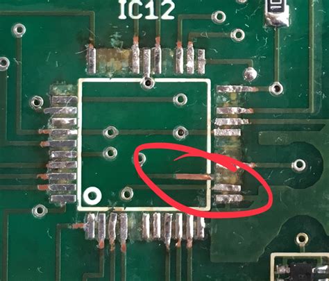
Tip 4: Repair Damaged Traces
PCB Traces are the conductive paths that connect components on the board. Sometimes, these traces can be damaged due to physical stress, corrosion, or overheating. Here’s how to repair damaged traces:
Jumper Wires
For small breaks or gaps in traces, jumper wires can be used to bridge the connection. Here’s how:
- Scrape away any Solder Mask or coating from the ends of the broken trace using a knife or scraper.
- Tin the exposed copper using a soldering iron and solder.
- Cut a piece of insulated wire (e.g., 30 AWG) to the appropriate length, leaving some slack.
- Strip the insulation from both ends of the wire.
- Solder one end of the wire to each end of the broken trace.
Conductive Epoxy
For more extensive damage or hard-to-reach areas, conductive epoxy can be used to repair traces. Conductive epoxy is a two-part adhesive filled with conductive particles, such as silver or carbon. Here’s how to use it:
- Clean the damaged area thoroughly with isopropyl alcohol.
- Mix the two parts of the epoxy according to the manufacturer’s instructions.
- Apply the epoxy to the damaged area using a fine-tipped applicator or toothpick.
- Allow the epoxy to cure according to the manufacturer’s instructions (usually 24-48 hours).
Tip 5: Protect and Reinforce the PCB
After completing the repairs, it is important to protect and reinforce the PCB to prevent future damage. Here are some methods:
Conformal Coating
Conformal coating is a protective layer applied to the PCB surface to shield it from moisture, dust, and other environmental factors. There are several types of conformal coatings, including:
- Acrylic
- Silicone
- Polyurethane
- Epoxy
Conformal coating can be applied using various methods, such as spraying, dipping, or brushing. It is important to follow the manufacturer’s instructions for application and curing.
Strain Relief
Strain relief is a method of reducing mechanical stress on the PCB and its components, particularly where cables or wires are connected. This can be achieved by using:
- Cable ties or clamps
- Strain relief connectors
- Adhesive-backed cable mounts
Proper strain relief helps prevent damage to the PCB traces and solder joints due to excessive bending or pulling of the cables.
Tip 6: Test and Validate the Repair
After completing the repair and protection steps, it is crucial to test and validate the PCB to ensure it functions as intended. Here are some steps to follow:
Visual Inspection
Perform a final visual inspection of the PCB, checking for any missed defects, poor solder joints, or damaged components.
Continuity Testing
Use a multimeter to verify the continuity of the repaired traces and connections.
Functional Testing
Test the PCB in its intended system or application to ensure it performs correctly under normal operating conditions.
Stress Testing
If possible, subject the PCB to stress tests, such as temperature cycling or vibration, to assess its durability and reliability.
Documentation
Document the repair process, including the problem, the steps taken, and the results of the testing. This can be valuable for future reference or troubleshooting.
Conclusion
PCB repair is a valuable skill for anyone working with electronics. By following these six tips, you can effectively diagnose, repair, and protect PCBs, saving time and resources. Remember to always prioritize safety, use the appropriate tools and techniques, and test thoroughly to ensure a successful repair.
Frequently Asked Questions (FAQ)
- What safety precautions should I take when repairing PCBs?
- Always wear safety glasses to protect your eyes from debris or splashes.
- Use a well-ventilated area or fume extractor when soldering to avoid inhaling fumes.
- Keep flammable materials away from the work area to prevent fire hazards.
-
Wear protective gloves when handling chemicals or cleaning agents.
-
Can I repair a PCB without schematics or documentation?
- While it is possible to repair a PCB without schematics or documentation, it can be much more challenging and time-consuming.
- Schematics and documentation provide valuable information about the PCB layout, components, and intended functionality.
-
If schematics are not available, you may need to rely on reverse engineering techniques, such as tracing circuits and comparing with similar designs.
-
How do I choose the right soldering iron for PCB repair?
- Consider the type of components you will be working with (through-hole or surface-mount).
- Look for a soldering iron with adjustable temperature control, as different components and solder types require different temperatures.
- Choose a soldering iron with a suitable wattage (usually 20-50 watts for PCB work).
-
Invest in a good quality soldering iron with replaceable tips for better performance and longevity.
-
Can I use regular super glue instead of conformal coating?
- No, regular super glue is not a suitable substitute for conformal coating.
- Conformal coatings are specifically designed for PCB protection and have properties such as electrical insulation, moisture resistance, and flexibility.
-
Super glue can be brittle, conductive, and may degrade over time, potentially causing more harm than protection to the PCB.
-
How can I prevent static damage when handling PCBs?
- Use an anti-static mat or wrist strap when working on PCBs to dissipate any static charges.
- Avoid wearing synthetic clothing, which can generate static electricity.
- Store PCBs in anti-static bags or containers when not in use.
- Discharge yourself by touching a grounded metal object before handling PCBs.
| Tool | Purpose |
|---|---|
| Soldering Iron | Melting solder to join components and traces |
| Multimeter | Testing continuity, voltage, and resistance |
| Isopropyl Alcohol | Cleaning PCBs and removing flux residue |
| Solder | Creating electrical and mechanical connections |
| Desoldering Pump | Removing solder from joints for component removal |
| Tweezers | Handling and placing small components |
| Magnifying Glass | Inspecting PCBs and components for defects |
| Solder Wick | Removing excess solder from joints |
| Flux | Improving solder flow and preventing oxidation |
| Conformal Coating | Protecting PCBs from environmental factors |
By having these essential tools and supplies on hand, you’ll be well-equipped to tackle a wide range of PCB repair tasks effectively and efficiently.
No responses yet