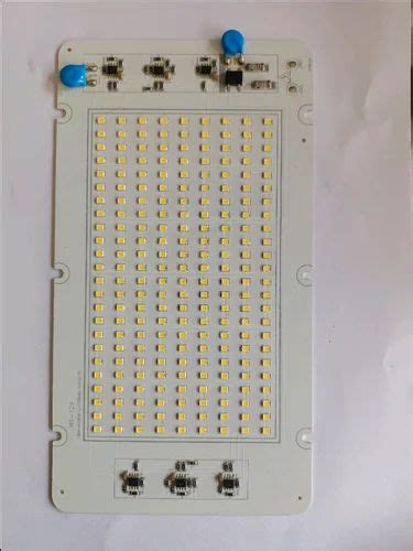
Introduction to LED PCB Assembly
Light-emitting diode (LED) printed circuit board (PCB) assembly is a crucial process in the manufacturing of LED lighting products. LED PCBs are designed to support and connect LED components, ensuring optimal performance and reliability. In this ultimate guide, we will delve into the intricacies of LED PCB assembly and discuss common defects and their analysis.
Key Components in LED PCB Assembly
1. LED Chips
LED chips are the heart of any LED PCB assembly. They are responsible for emitting light and come in various sizes, colors, and power ratings. Proper selection and placement of LED chips are essential for achieving the desired luminous output and energy efficiency.
2. PCB Substrate
The PCB substrate serves as the foundation for the LED assembly. It is typically made of FR-4, a flame-retardant material composed of fiberglass and epoxy resin. The substrate provides mechanical support and electrical insulation for the LED components.
3. Thermal Management
Effective thermal management is crucial in LED PCB assembly to ensure optimal performance and longevity of the LED components. Heat sinks, thermal interface materials (TIMs), and proper PCB design techniques are employed to dissipate heat generated by the LEDs.

LED PCB Assembly Process
1. Solder Paste Printing
The first step in LED PCB assembly is the application of solder paste onto the PCB pads using a stencil or screen printing process. Solder paste is a mixture of tiny solder balls and flux, which helps to establish electrical and mechanical connections between the components and the PCB.
2. Component Placement
After solder paste printing, the LED components are placed onto the PCB using pick-and-place machines. These automated systems accurately position the components based on the PCB design files, ensuring precise alignment and orientation.
3. Reflow Soldering
Once the components are placed, the PCB undergoes a reflow soldering process. The assembly is heated in a controlled manner, causing the solder paste to melt and form reliable solder joints between the components and the PCB pads. The temperature profile is carefully controlled to prevent damage to the components and ensure optimal solder joint formation.
4. Inspection and Testing
After the reflow soldering process, the LED PCB assembly undergoes rigorous inspection and testing to ensure quality and functionality. Automated Optical Inspection (AOI) systems are used to detect any visible defects, while functional testing verifies the electrical performance and light output of the LED assembly.

Common Defects in LED PCB Assembly
1. Solder Bridges
Solder bridges occur when excess solder inadvertently connects adjacent pads or components, creating unintended short circuits. These defects can lead to malfunction or complete failure of the LED assembly.
2. Cold Solder Joints
Cold solder joints are a result of insufficient heat during the soldering process, leading to poor solder wetting and weak mechanical connections. These joints are prone to cracking and can cause intermittent or complete failure of the LED assembly.
3. LED Misalignment
Misalignment of LED components can occur due to improper placement or shifting during the reflow soldering process. Misaligned LEDs can result in uneven light distribution, reduced luminous output, and potential damage to the components.
4. Tombstoning
Tombstoning is a defect where a surface-mount component, such as an LED, stands up on one end due to uneven heating or solder wetting. This defect can cause open circuits and compromise the reliability of the LED assembly.

Defect Analysis Techniques
1. Visual Inspection
Visual inspection is the first line of defense in identifying defects in LED PCB assembly. Trained operators use magnification tools and lighting to examine the assembly for visible anomalies such as solder bridges, misaligned components, and discoloration.
2. X-Ray Inspection
X-ray inspection is a non-destructive technique used to detect hidden defects within the LED assembly, such as voids in solder joints or misaligned internal components. This method provides a detailed view of the internal structure of the assembly without the need for disassembly.
3. Thermal Imaging
Thermal imaging is used to analyze the thermal performance of the LED assembly. By capturing infrared images of the PCB during operation, engineers can identify hot spots, uneven heat distribution, and potential thermal management issues.
4. Electrical Testing
Electrical testing is performed to verify the functionality and performance of the LED assembly. This includes measuring forward voltage, luminous flux, color temperature, and other relevant parameters to ensure compliance with specifications.
Best Practices for LED PCB Assembly
- Use appropriate solder paste and stencil design to ensure optimal solder joint formation.
- Implement robust pick-and-place processes to minimize component misalignment and damage.
- Optimize reflow soldering profiles based on the specific requirements of the LED components and PCB materials.
- Conduct thorough inspection and testing at various stages of the assembly process to identify and rectify defects early.
- Employ effective thermal management techniques, such as proper heat sink design and thermal interface materials, to ensure optimal LED performance and longevity.
Frequently Asked Questions (FAQ)
1. What is the difference between through-hole and surface-mount LED PCB assembly?
Through-hole LED PCB assembly involves inserting LED leads through holes in the PCB and soldering them on the opposite side. Surface-mount LED PCB assembly, on the other hand, involves placing LED components directly onto the PCB surface and soldering them using reflow techniques. Surface-mount assembly is more common in modern LED manufacturing due to its higher density and automated processes.
2. Can LED PCB assembly be done manually?
While it is possible to perform LED PCB assembly manually, it is not practical for large-scale production. Manual assembly is time-consuming, labor-intensive, and prone to human error. Automated processes, such as pick-and-place machines and reflow soldering, are preferred for their speed, accuracy, and consistency.
3. How can I prevent solder bridges in LED PCB assembly?
To prevent solder bridges, ensure that the solder paste is applied accurately using a well-designed stencil. Optimize the solder paste printing process to maintain consistent solder volume and avoid excessive solder deposition. Additionally, proper component placement and reflow soldering profile control can help minimize the occurrence of solder bridges.
4. What is the importance of thermal management in LED PCB assembly?
Proper thermal management is crucial in LED PCB assembly because LEDs generate a significant amount of heat during operation. Excessive heat can lead to reduced luminous output, color shift, and premature failure of the LED components. Effective thermal management techniques, such as using heat sinks and thermal interface materials, help to dissipate heat and maintain optimal LED performance and longevity.
5. How can I ensure the quality of LED PCB assembly?
To ensure the quality of LED PCB assembly, implement a comprehensive quality control process that includes:
– Incoming material inspection to verify the quality of components and PCBs.
– Process control and monitoring to maintain consistent assembly parameters.
– Automated optical inspection (AOI) to detect visible defects.
– X-ray inspection to identify hidden defects in solder joints and internal components.
– Functional testing to validate the electrical and optical performance of the LED assembly.
– Continuous improvement initiatives to identify and address root causes of defects and optimize the assembly process.
Conclusion
LED PCB assembly is a complex process that requires precision, expertise, and attention to detail. By understanding the key components, assembly process, common defects, and analysis techniques, manufacturers can ensure the production of high-quality LED lighting products. Implementing best practices and utilizing advanced technology in LED PCB assembly can lead to improved efficiency, reliability, and customer satisfaction in the rapidly growing LED lighting industry.
No responses yet