Introduction to PCB Design
Printed Circuit Board (PCB) design is a crucial aspect of electronic product development. It involves the creation of a layout that connects electronic components on a board, enabling them to function as intended. PCB design services encompass various stages, from schematic capture to final board layout, ensuring that the resulting PCB meets the required specifications and performs optimally.
The Importance of PCB Design
PCB design plays a vital role in the success of an electronic product. A well-designed PCB ensures:
- Reliability: Proper PCB layout minimizes signal interference, reduces electromagnetic compatibility (EMC) issues, and enhances the overall reliability of the product.
- Functionality: Accurate PCB design ensures that all components are connected correctly, enabling the product to function as intended.
- Manufacturability: A well-designed PCB layout considers manufacturing constraints, such as component placement, trace width, and spacing, making it easier to fabricate and assemble the board.
- Cost-effectiveness: Efficient PCB design optimizes the use of board space, minimizes the number of layers required, and reduces the overall cost of the product.
PCB Design Process
The PCB design process typically involves the following stages:
1. Schematic Capture
Schematic capture is the first step in PCB design. It involves creating a graphical representation of the electronic circuit using specialized software. The schematic diagram shows the interconnections between components and provides a clear understanding of the circuit’s functionality.
2. Component Selection
Once the schematic is complete, the next step is to select the appropriate components for the PCB. This involves considering factors such as:
- Electrical specifications (e.g., voltage rating, current rating, tolerance)
- Physical dimensions
- Availability and cost
- Reliability and durability
3. PCB Layout
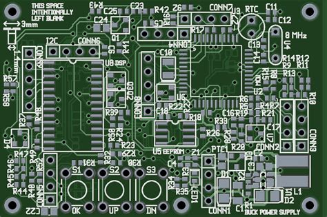
After component selection, the PCB layout process begins. This stage involves arranging the components on the board and routing the traces to connect them according to the schematic diagram. PCB layout software is used to create the layout, which typically includes the following steps:
-
Component Placement: Components are positioned on the board based on their functional requirements, physical dimensions, and manufacturing constraints.
-
Routing: Traces are routed to connect the components according to the schematic diagram. The routing process considers factors such as signal integrity, EMC, and manufacturability.
-
Design Rule Check (DRC): A DRC is performed to ensure that the PCB layout adheres to the design rules specified by the manufacturer. This includes checking for minimum trace width, spacing, hole sizes, and other parameters.
4. PCB Fabrication
Once the PCB layout is finalized and verified, the design files are sent to a PCB fabrication house for manufacturing. The fabrication process involves the following steps:
-
PCB Printing: The PCB layout is printed onto a copper-clad substrate using photolithography or other imaging techniques.
-
Etching: The unwanted copper is removed from the substrate, leaving behind the desired traces and pads.
-
Drilling: Holes are drilled into the board for component mounting and via connections.
-
Surface Finish: A surface finish, such as solder mask and silkscreen, is applied to protect the copper traces and improve solderability.
5. PCB Assembly
After fabrication, the PCB is ready for assembly. This stage involves soldering the components onto the board according to the assembly drawing. The assembly process can be done manually or using automated equipment, depending on the complexity of the board and the production volume.
PCB Design Considerations
To ensure a successful PCB design, several key factors must be considered:
1. Signal Integrity
Signal integrity refers to the quality of the electrical signals transmitted through the PCB. Factors that can affect signal integrity include:
- Trace length and impedance
- Crosstalk between adjacent traces
- Reflections due to improper termination
- Electromagnetic interference (EMI)
To maintain signal integrity, designers must carefully select the appropriate trace width, spacing, and routing techniques. Additionally, proper grounding and shielding techniques should be employed to minimize EMI and crosstalk.
2. Thermal Management
Thermal management is critical in PCB design, especially for high-power applications. Excessive heat can lead to component failure and reduced reliability. To mitigate thermal issues, designers can:
- Select components with appropriate power ratings
- Use thermal vias to dissipate heat from components to the PCB’s copper layers
- Incorporate heatsinks or other cooling solutions
- Optimize component placement to promote airflow and heat dissipation
3. Manufacturability
Designing a PCB with manufacturability in mind is essential for ensuring a smooth and cost-effective production process. Key considerations include:
- Adhering to the manufacturer’s design rules and guidelines
- Minimizing the number of PCB Layers to reduce cost
- Using standard component sizes and packages
- Providing adequate clearance for component placement and soldering
- Incorporating fiducial markers and alignment holes for automated assembly
4. Testing and Debugging
Designing a PCB with testability in mind can greatly simplify the debugging process and reduce development time. Strategies for improving testability include:
- Incorporating test points and probe pads for access to critical signals
- Using boundary scan techniques for testing complex digital circuits
- Providing clear silkscreen labels and component designators
- Including provisions for in-circuit programming and firmware updates

PCB Design Software
There are numerous PCB design software packages available, ranging from free, open-source tools to high-end commercial solutions. Some popular options include:
| Software | Vendor | Key Features |
|---|---|---|
| Altium Designer | Altium | Comprehensive PCB design suite with 3D modeling and simulation capabilities |
| KiCad | KiCad | Free and Open-source PCB design software with schematic capture, layout, and 3D viewing |
| Eagle | Autodesk | Widely used PCB design software with a large component library and community support |
| OrCAD | Cadence | Powerful PCB design solution with advanced simulation and analysis tools |
When selecting a PCB design software, consider factors such as ease of use, availability of component libraries, integration with other tools, and cost.
PCB Layout Techniques
Effective PCB layout techniques are essential for ensuring a reliable and high-performance design. Some key techniques include:
1. Ground Planes
Using a solid ground plane is one of the most effective ways to improve signal integrity and reduce EMI. A ground plane provides a low-impedance return path for signals and helps to shield sensitive traces from external noise.
2. Power Planes
Similar to ground planes, power planes provide a low-impedance distribution network for power supply voltages. By using dedicated power planes, designers can minimize voltage drops and ensure a stable power supply to all components.
3. Differential Pairs
Differential signaling is a technique used to transmit high-speed signals while minimizing noise and crosstalk. By routing differential pairs closely together and maintaining a constant spacing between the traces, designers can ensure that any noise induced on one trace is canceled out by the opposite signal on the other trace.
4. Trace Routing
Proper trace routing is critical for maintaining signal integrity and minimizing crosstalk. Some guidelines for trace routing include:
- Keeping trace lengths as short as possible
- Avoiding sharp bends and corners
- Maintaining consistent trace width and spacing
- Using 45-degree angles for trace bends
- Avoiding crossing traces on the same layer
5. Component Placement
Optimal component placement can greatly simplify the PCB layout process and improve the overall performance of the design. Guidelines for component placement include:
- Grouping components by function and connectivity
- Minimizing the distance between connected components
- Placing sensitive components away from sources of noise
- Orienting components to facilitate trace routing
- Providing adequate clearance for soldering and assembly
Frequently Asked Questions (FAQ)
1. What is the difference between a schematic and a PCB layout?
A schematic is a graphical representation of an electronic circuit, showing the interconnections between components. A PCB layout, on the other hand, is the physical arrangement of components and traces on a printed circuit board.
2. How do I choose the right PCB Manufacturer?
When selecting a PCB manufacturer, consider factors such as:
– Experience and reputation
– Quality control processes
– Turnaround time and pricing
– Capabilities (e.g., number of layers, minimum trace width, hole sizes)
– Customer support and communication
3. What is the purpose of a design rule check (DRC)?
A design rule check (DRC) is a process that verifies that a PCB layout adheres to the design rules specified by the manufacturer. This includes checking for minimum trace width, spacing, hole sizes, and other parameters. The purpose of a DRC is to ensure that the PCB can be manufactured reliably and cost-effectively.
4. How can I minimize electromagnetic interference (EMI) in my PCB design?
To minimize EMI in a PCB design, consider the following strategies:
– Use a solid ground plane to provide shielding and a low-impedance return path
– Route sensitive traces away from sources of noise, such as power supplies and high-speed digital signals
– Use differential signaling for high-speed signals
– Incorporate EMI filters and shielding components, such as ferrite beads and metal enclosures
5. What are the advantages of using a four-layer PCB over a two-layer PCB?
A four-layer PCB offers several advantages over a two-layer PCB, including:
– Improved signal integrity due to the use of dedicated power and ground planes
– Reduced electromagnetic interference (EMI) and crosstalk
– Increased routing density and flexibility
– Better thermal management due to the additional copper layers
However, four-layer PCBs are more expensive to manufacture than two-layer PCBs, so designers must weigh the benefits against the added cost.
Conclusion
PCB design is a complex and iterative process that requires a deep understanding of electronic circuits, manufacturing processes, and design principles. By following best practices for component selection, schematic capture, PCB layout, and manufacturability, designers can create reliable, high-performance PCBs that meet the requirements of their applications.
Investing in the right PCB design software, partnering with experienced manufacturers, and staying up-to-date with the latest design techniques and technologies are key to success in this field. With the growing demand for electronic products across industries, the importance of skilled PCB designers and reliable PCB design services will only continue to increase in the years to come.

No responses yet